
How to Switch Large Loads with a Microcontroller Using Transistors
Microcontrollers are great for implementing the smarts behind a given product. This article teaches you how to get around some of their major limitations.

One thing that microcontrollers cannot do is directly control anything other than, maybe, a single LED. That’s because the output drive of most microcontrollers can directly source or sink only about 10mA.
Let’s look at several ways to switch heavier loads on the low side from a typical microcontroller output. A few simple math calculations are required to determine typical component values, and these will be presented in easily accessible formats. However, this approach means that some liberties have been taken with technical rigors.
One of the simplest approaches to controlling large loads that operate on DC current is the saturated switch. The actual electronic switch element comes in two variants: Bipolar Junction Transistors, or BJTs, and MOSFETs.
Before getting to the actual switch itself, let’s define what is meant by low-side switching. Figure 1 shows this type of load switching.
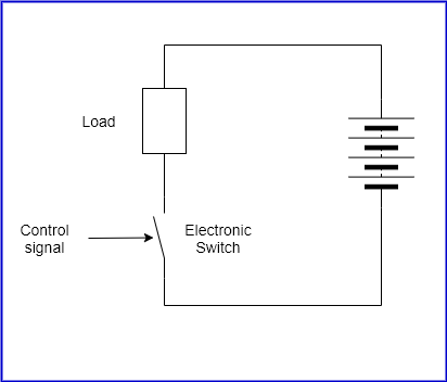
Figure 1 – Low-side load switch
The switch controls the negative side of the load. This means that when the switch is open, the load is essentially floating with respect to the negative of the power supply, which is usually the ground reference in most designs.
If this type of switching arrangement is acceptable, then the low-side switch is usually the cheapest way to achieve load switching.
BJT Low-Side Switch
A BJT can be used as a load switch and come in two flavors: NPN and PNP. For low-side switching, NPN transistors are used, and for high-side switching a PNP is used.
Before getting into the actual methods, let’s define some nomenclature that are used when dealing with NPN transistors.
Figure 2 shows the pertinent voltage and current naming conventions. Starting with the current, IB is the base current, and is shown entering the base of the NPN. The same arguments apply for IC and IE, with IE shown leaving the transistor.
It can be seen that: IE = IC + IB
With the voltages, VCE is the voltage between the Collector and the Emitter, and is generally a positive value for NPN transistors. In other words, for the NPN transistor the collector voltage is generally higher than the emitter voltage.
Following the same convention, VBE is the voltage between the Base and the Emitter. It is generally positive for NPN’s.
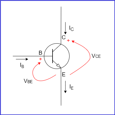
Figure 2 – NPN BJT voltage and current
The key to understanding how a transistor can control a large load is this equation:
IC = βIB, where β is the DC current gain, and is maybe 20 to as high as 300, or more.
This says that the Collector current is the β value times the Base current. So, if β = 100, then the Collector current will be 100X the base current.
The value of β is given in the datasheet of a given transistor as hFE. For the purpose of this article, they mean the same thing. Note that it is not a fixed value for a given transistor, but varies somewhat with the value of the Collector current and temperature, but that will not matter much for the purpose of this article.
When BJT’s are used as load switches, they are used in two modes: Cutoff and Saturation. Consider figure 3 below. As previously stated, IC = βIB. So, if IB = 0, then IC must also be 0. In this state, the transistor is in cut-off mode. Note that since no current is flowing in the transistor, it isn’t dissipating any power; also in this case, VC is the same as VCC.
For the next part, assume that VCC = 10 Volts, R = 10Ω, and β = 100. Let’s see what happens when IB = 1mA. In this case, IC = 100mA, since β = 100. The voltage across the resistor is IC x RL, or 1V. This implies that VC must be 9V then, since VCC is 10V, and the voltage drop across RL is 1V. The same argument applies if IB = 2mA, and so on.
Now, what happens if IB = 20mA. According to the calculations, this implies that IC = 2000mA, or 2A. However, this cannot be the case. Since VCC = 10 Volts and RL = 10Ω, the maximum current that can flow through RL is 1A.
In other words, the maximum value of IC is also 1A. This occurs when VC = 0, meaning that the transistor is a dead short to ground.
In this state, the transistor is said to be in saturation mode. In this mode, the transistor collector current is the maximum that the circuit conditions allow, and increasing base current will not cause it to go any higher.
So, the equation IC = βIB only holds until the transistor is saturated. Note that if, in the example just described, VCC is now increased to, say, 25V, or RL is changed to 1Ω, the transistor will no longer be saturated. Thus, saturation is defined in relation to external circuit conditions.
Finally, note that real transistors cannot be complete short circuits between their collectors and emitters unless they are defective. When a real transistor is saturated its VCE will be at a value of VCEsat. This value is given in the transistor datasheet, and is usually between 0.2V for a small transistor to more than 1V for a large one.
VCEsat is also dependent on the collector current and the temperature. This dependence is typically given as a set of curves in the datasheet.
In saturation mode, the transistor is dissipating some power, given by
Power dissipated = IC x VCEsat
However, since VCEsat is usually quite low, the power dissipation will also be low. Thus, cut-off and saturation are the two states where the transistor will be dissipating the lowest power.
Focusing now on the Base of the transistor, a quick way to set IB is to assume VBE is 0.7V. This value works for most transistors.
So, in this case, by Ohm’s Law,
If a given value of IB is needed, then RB can be calculated as:
RB = (VBB – 0.7) / IB
In order to saturate the transistor, the minimum IB required is the value that will cause the maximum IC, given the β value of the transistor and the circuit conditions.
In practice, this IB value should be greater than this minimum by about 10% to 15% to account for device to device variations of the β value.
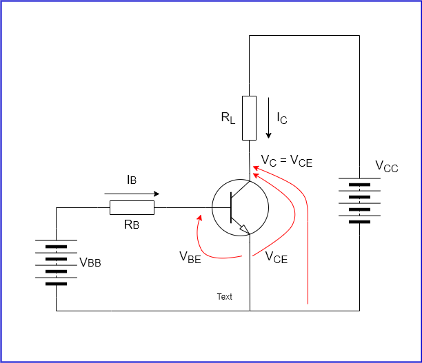
Figure 3 – Transistor operation
Driving a BJT from a microcontroller
What was just described is actually a low-side NPN BJT switch. If VBB were the output pin of a microcontroller, then knowing its logic high value, the required load current and the transistor β value, the value of RB can easily be calculated.
A few other things to check are to make sure that:
The calculated IB does not exceed the drive current capability of the microcontroller.
The load current does not exceed the maximum collector current of the transistor.
The power dissipation in saturation mode does not exceed the maximum power dissipation of the transistor.
The VCC voltage does not exceed the maximum VCE of the transistor.
Some safety and derating margins should also be incorporated in the above example to ensure reliable operation. About 20% is reasonable.
Driving heavier loads using a Darlington
Since the drive current of a microcontroller GPIO pin rarely exceeds 10mA, and transistor minimum β typically does not exceed around 50 for a power transistor, then the most current that can be controlled is about 500mA.
In order to be able to control higher currents, a Darlington arrangement can be employed. There are Darlingtons available in a single package, or it can be made up using two transistors as shown in figure 4.
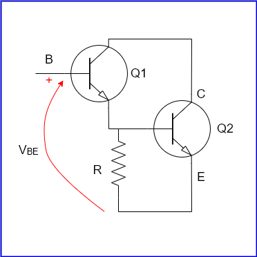
Figure 4 – NPN Darlington
In this arrangement, Q1 is generally a low power high gain transistor, and Q2 is a high-power transistor. Assuming that the resistor R is not present for the moment, then it is seen that all the Q1 emitter current flows into the base of Q2.
As previously stated, emitter current is the sum of the Collector current and the Base current.
Thus, IE = β x IB + IB, or IE = (β + 1) IB
Since β is quite large, (β + 1) is close to β.
This means:
IE ≈ IC
Now, since IE of Q1 flows directly into the Base of Q2, that means the IC2, the collector current of Q2 is given by:
So, a small input base current can produce a large output collector current. There are a few issues to note though. First, the VBE of this composite transistor is now the sum of the VBE’s of the two transistors. This has to be taken into account when base resistor value is calculated as detailed before.
As for the resistor R, it affects the turn-off time of Q2. When Q2 is conducting, it has charges flowing into its Base. Now, when the input to Q1 goes low, Q1 turns off, and the charge stored in the Base of Q2 has nowhere to go.
It will eventually disappear by an internal process called carrier recombination, but until that happens, Q2 will remain in a conducting state. This can last from a few microseconds to tens of microseconds depending on the transistor.
In essence, the microcontroller turns off its output, but the load remains on for a bit of time after. R is used to speed up the turn-off of Q2 by bleeding off the stored base charge.
For applications such as PWM, it is thus recommended to use this resistor. For most embedded applications, values between 1KΩ and 5KΩ work fine.
R also shunts some of the base current of Q2 under normal operation. This current is (VBE2 / R), or approximately 0.7/R. To offset this current, just increase the base current of Q1. Since this Base current x β1 must be equal to 0.7/R, it follows that the base current in Q1 should be increased by (0.7/ (β1 x R)).
MOSFET Low-Side Switch
As with the BJT, a MOSFET comes in two basic flavors: N-Channel and P-Channel. The N-Channel MOSFET is similar to an NPN and is used for low-side switching. Likewise, the P-Channel MOSFET is similar to an PNP BJT, and is used for high-side switching.
The N-Channel enhancement MOSFET is relatively easy to interface to a microcontroller GPIO output pin, subject to certain conditions being met.
Figure 5 shows this type of MOSFET, together with some of its more important aspects when this device is being considered as a low-side switch.
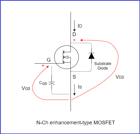
Figure 5 – N-Channel enhancement MOSFET
When a voltage is applied between the Gate and the Source, a current will begin to flow between its Drain and Source if the voltage is higher than a threshold voltage, Vth, that is given in its datasheet.
Above that threshold value, the higher the VGS is, the larger the Drain current ID is, until VGS reaches VGSMax, again given by the datasheet. ID vs VGS is given by a set of curves in the datasheet, and, as in the BJT case, the MOSFET is saturated when the drain current is the maximum that the circuit conditions allow.
Since the MOSFET is a voltage-controlled device, it requires almost no current to keep it turned on. So, a GPIO from a microcontroller can drive a MOSFET that can then control very large currents. There is no need for Darlington arrangements. MOSFETS with low Vth that are fully enhanced at 5V Gate drive are available that can, in turn, control several amps.
Another advantage of the MOSFET over the BJT is that there is no VDSsat. Instead, when the MOSFET is conducting, the Drain-Source connection behaves like a resistor with a value of RDS that is a function of VGS, and can be a very low value for a power MOSFET.
Thus, the power dissipation of the MOSFET when it is conducting, or enhanced, is simply the value of (ID)2, where ID is the drain current, multiplied by the RDS, the same as the power dissipated in a resistor, R, passing a current, I, is given by P = I2R.
So, in many circumstances the power dissipated by a saturated MOSFET will be less than that by an equivalent BJT. This is especially true if ID is fairly high.
One thing to note is that all N-Ch MOSFETS have built-in substrate diodes as shown in figure 5. This is inherent in the construction of the MOSFET. Practically, what this means is that the Drain must be more positive than the Source; otherwise this diode will conduct.
Finally, one big issue with MOSFETs is the Gate-Source capacitance. It can be quite large for a power MOSFET – 3nF or more is not uncommon. Practically, what this means is that before the MOSFET can start conducting, this Gate capacitance must charge up first. Given that most microcontrollers can source limited current, it will take time for this capacitor to charge up.
So, when driven directly by the output of a microcontroller, the MOSFET simply cannot switch very fast. So, using the MOSFET for fast PWM will probably not work.
In such situations, a MOSFET driver such as the TI UCC27511, must be used between GPIO pin and the Gate of the MOSFET. This, of course, adds even more cost to the already higher cost of a MOSFET over a BJT.

Hi,
I found this article really helpful, i have designed a switch based on the mosfet circuit. It works perfectly fine but at the time when i turn power ON, then for very small time period(when the processor is being reset) switch turns ON automatically. Can you please help me out?
Try a drain resister 10k to ground between controller and base?
This article is good, but I think it lacks a description of the difference of low-side vs. high-side switch (since you point it out that it’s obviously a difference).
Instead of a Darlington pair with its large VBE one might want to consider the Sziklai pair.
Both the Darlington and Sziklai are problematic when used as switches. As discussed at https://sound-au.com/articles/cmpd-vs-darl.htm and illustrated in his Figure 2, have saturation (on) voltage drops that are much higher than appropriately rated BJT or MOSFET switches. This causes heating, of course, and often the need for a heatsink if the switched current is 1 A or more. Given that modern MOSFETs have become very inexpensive, they are the “device of choice” in modern circuit design. But the Sziklai configuration can make an excellent amplifier (or voltage follower/buffer) with very low noise (depending mostly on the input side transistor) and extremely high effective h-sub FE. I’ve used them for over 40 years, but never heard them called by that name!
good one
Useful tutorial for beginners, but it would be more useful if you tell to your audience about the needing to put a diode on inductive loads. A beginner could connect a rele without diode and destroy its transistor, asking why…
I think it’s important to point out that the diode used to suppress the “inductive kick” or back-EMF when a relay coil is switched off also significantly slows the relay’s turn-off (or “dropout”) time. If a fraction of a second delay is important in your application, a better solution is to use a high-voltage driver (say a 400 V rated MOSFET) and reduce the peak voltage “kick” with a resistor. The value of the resistor is best determined experimentally using an oscilloscope and starting with a resistor value equal to the relay’s coil resistance. Note that the “dropout time” listed in a relay spec sheet is without the diode!
i don’t get it. How does a diode stretch the dropout time? and how do they measure dropout time without a diode?
The relay coil has a lot of inductance. If you suddenly stop current flow in an inductor, the magnetic field collapses. It’s that rapid collapse that (as predicted by Faraday’s law) induces a very high voltage in the coil. If we put a diode across the coil to suppress this back-EMF, we’re allowing current to continue flowing in the coil, which keeps the contacts closed, until the energy is dissipated (as heat) in the relay coil. Without the diode, the back-EMF can easily reach hundreds of volts (depends on a number of factors but most important is the metal structure of the relay that acts as a shorted turn to eddy currents induced by the rapid collapse of the magnetic field). Here is a useful document by Panasonic about the use of relays: https://www.panasonic-electric-works.com/pew/eu/downloads/ds_x61_en_relay_technical_information.pdf. To quote from page 24, “Connection of a diode is an excellent way to prevent voltage surges, but there will be a considerable time delay when the relay is open. If you need to reduce this time delay you can connect between the transistor’s collector and emitter a Zener diode that will make the Zener voltage somewhat higher than the supply voltage.” The English is a bit awkward, but it makes the point. In the book Self on Audio: The Collected Audio Design Articles of Douglas Self, he measures the drop-out time of some commercial relays – using the diode typically multiplies rated times by 5 to 7 times!
I’m currently designing a power-line surge suppressor that can rapidly sense (actually predict) an incoming AC over-voltage (such as being connected to 240 VAC at a faulty 120 V outlet). It’s important that the relay disconnect in less that 1/2 cycle of 60 Hz – so my design uses a relay with dropout time of 4 milli-seconds to rapidly disconnect protected equipment. In my design, the relay has a 48 VDC coil, but I’m driving it with a small MOSFET rated for 600 V and using a 400 V zener diode from drain to source to protect the MOSFET. Diodes across DC relay coils is one of those things that most engineers do without a second thought, but years of experience teach us many things you don’t learn in college!
wow i never thought about it either. so you’re saying that if the voltage rises to 400v then the energy will dissipate that much faster than it will at only .7v?
One way to look at this, based on Bill’s explanation, is that you want to get the energy out of the coil as fast as possible after power to it is disconnected. Since resistance in the coil and a connected protection diode is low, it takes time for the energy in the coil to dissipate, and all the while it still has an active magnetic field holding the relay in its on-state. However, with the zener mentioned by Bill, together with a load resistor in series with it that turns on only when the field is collapsing, that energy can be bled off much faster. The zener is used to control the maximum voltage that develops across the transistor. Another option is create a “snubber” which is a tuned resistor and capacitor connected across the transistor, such that the energy from the coil is transferred to the capacitor and then dissipated by the resistor. The snubber has to be tuned carefully to achieve your goal of protecting the transistor, so a zener (or “Transient Voltage Suppressor” device) is less complicated to use.
Another huge consideration is EMI – electromagnetic interference. The relay’s collapsing magnetic field generates a huge voltage pulse. That pulse, when it discharges through a diode, creates radio waves at a wide spectrum of frequencies since the attack (rise time) of the current is fast (and Fourier theory says that a rapid change includes high frequencies.) This energy spreads out through your ground connections as well as through the air, and can disrupt other circuits in your design. The snubber can reduce the speed of the voltage change which reduces the frequency of the radiated emissions. The zener approach can reduce the size of the voltage spike which can also be useful to reduce EMI.
In my most recent design I gave up on mechanical relays completely. They were sending noise back into my system both due to their own coils and the coils in equipment they were switching on and off. Instead I used solid state relays which don’t have an inductive kick, and can be purchased or set up to switch at current zero-crossings, so the loads they switch don’t generate inductive spikes. However, your application will decide for you which one works best.
How about digital FETs like FDV303N or similar, no need for a MOSFET driver?
Excellent question! The FDV303N is a perfect example of a “low-threshold” MOSFET that is driven fully on by the 3.3 V high-level output voltage of popular micro-controllers. Most MOSFETs have higher gate threshold (threshold being the gate voltage where the MOSFET just begins to conduct drain current) voltages of 5 or even 10 V. If these higher-threshold parts are driven at 3 V, they may not turn on at all, or be only partially on, which makes them generate a lot of heat, potentially burning them up. When looking for suitable MOSFET switches, search for parts that are rated to switch the load current at the available gate drive voltage or lower. For example, the FDV303N datasheet says “RDS(ON) = 0.6 ohm @ VGS= 2.7 V”. If this RDS(on) spec lists a VGS higher than the supply voltage for your micro-controller, it won’t be a good candidate as your load switch! If you can’t find such a low-threshold device, you’ll have to design a “driver” to translate the controller’s output to a higher gate-drive voltage that’s typically required for very high current (say 5 A or more) loads.