
Introduction to Switch Mode Power Supply Design
This article provides an easily understandable approach to explaining how a switch-mode, buck or boost, power supply operates.

Most makers or enthusiasts know what a boost or buck converter does, and have used them before. However, they typically just follow a canned approach to designing one without fully appreciating exactly what it is doing.
Let’s look closer at how a switch-mode, buck or boost, power supply operates. The goal is not to provide detailed design information about these types of power supplies, but rather to understand its operation well enough to make informed decisions on the required aspects of such circuit blocks. So, the math and any design equations will be kept to a minimum.
Also, there are many Switch-Mode Power Supply, or SMPS, power supply topologies. To keep with the philosophy of this article, the discussions will be limited to simple boost or buck designs.
Fundamental Components
Before getting to how an actual SMPS works, this section briefly goes over some of the fundamental components of a typical SMPS.
The electronic switch
All switching power supplies require an electronically-controlled switch. The two most commonly used devices in low-power SMPS are the bipolar NPN transistor, and the N-Ch MOSFET. Figure 1 shows these two types of switches.
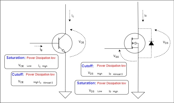
Figure 1 – Two common types of electronic switches used in simple SMPS circuits
The key thing to note here is that these switches are operated in saturation mode: either fully saturated of fully cut-off. In both of these cases, the power dissipation in the switch is minimized. This is, in fact, how switching power supplies achieve their high efficiencies compared to linear regulators.
Capacitors and inductors
Even though in a switch-mode power supply the inductor is the circuit element that plays the most significant role in its basic operation, this section will start with a review of some of a capacitor’s key operational features as this is conceptually easier to understand. This sets the stage for a better understanding of the inductor’s contribution.
Consider the circuit consisting of a fully-discharged capacitor charging up from a voltage source as shown in figure 2. When the switch closes, the capacitor voltage exponentially rises toward the battery voltage V, while the current exponentially decreases.
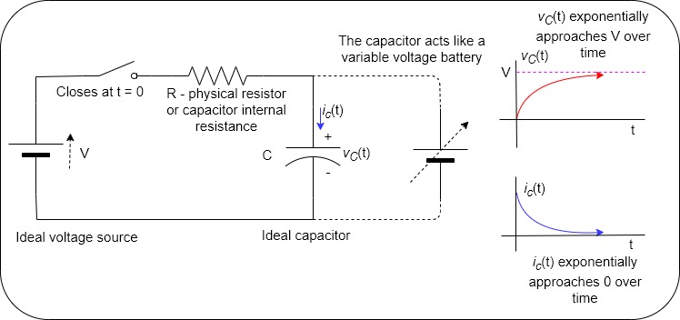
Figure 2 – Capacitor being charged from a voltage source
Note that to be technically correct, the capacitor voltage will never reach the same value as the battery voltage, and the current never drops all the way to zero. However, for all practical purposes, they eventually get close enough to their respective limits to be considered equal.
Also note that when the switch closes, the capacitor current instantly rises to a value that is actually equal to V/R. The voltage, on the other hand, rises slowly toward a value of V.
Now, consider the circuit in figure 3 below. When the switch S1 is closed, the capacitor will charge up as usual.
Now, if at some later time (T) the switch S1 is opened, and S2 is simultaneously closed then voltage across the capacitor will be at some voltage VOPEN which will depend on how long the capacitor has been charging up, prior to the switch opening.
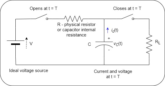
Figure 3 – Capacitor charge and discharge
This same voltage will now be across R, causing a current to flow through R, equal to VOPEN/R at the instant the switches are toggled.
The capacitor will, of course, discharge, giving up some of its stored energy, and the voltage across R will decrease as will the current. The thing to note here is that capacitor current has instantaneously reversed.
So, instead of flowing into the capacitor as when switch S1 was closed, it is now flowing out of the capacitor. The voltage across the capacitor, however, has not reversed.
Now moving on to inductors, figure 4 shows an inductor being driven by a constant voltage source – a battery. It is similar in many ways to the capacitor, except that the current and voltage curves are exchanged.
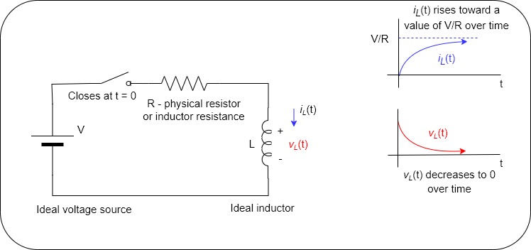
Figure 4 – Inductor being driven by a constant voltage source
The maximum current that can be eventually reached will be limited by the DC resistance of the wire that the inductor is made of, plus any actual physical resistor in the series circuit, and the battery voltage.
Figure 5 shows what happens when switch S1 is opened for an inductor that has been “charging” for a while. In a somewhat similar fashion to the capacitor case, but with the current and voltage roles exchanged, the voltage across the inductor instantaneously reverses so as to keep the same current flowing at the exact moment when the switches are toggled.
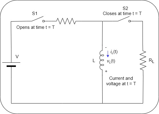
Figure 5 – Inductor driving a load
Again, to draw a parallel with the capacitor, this time it’s the inductor voltage that has changed direction while the current direction has stayed the same. Also, as in the case of the capacitor, the voltage and current will slowly drop as the inductor gives up its stored energy.
The Boost (Step-up) Converter
With the previous descriptions of the major components found in a typical SMPS, the operation of the boost converter can now be understood. This is shown in figure 6.
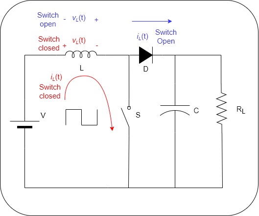
Figure 6 – Block diagram of a boost converter
As shown, the switch is an electronic switch such as an N-channel MOSFET that is continuously being closed or opened. When closed, the rising inductor current flows through the switch, and the inductor voltage slowly falls, but it is again in opposition to the battery voltage during this period.
When opened, as shown before, the voltage across the inductor instantaneously changes direction to try to keep the current flowing. This inductor current must flow through the diode D into the load since the switch is opened.
Note that the inductor voltage is now added to the battery voltage, so the output voltage will be higher than the battery voltage. Thus, boost converter action is achieved.
Also note that the current that was initially flowing in the inductor when the switch was closed will depend on how long the switch was closed. This current will be used to charge the capacitor and it also flows into the load.
By controlling the inductor current, the capacitor voltage, and hence the load voltage, can also be controlled. In other words, by controlling the ON time of the switch, the voltage at the load can be controlled.
The Buck (Step-down) Converter
The basic buck converter consists of the same components as the boost, but they are arranged differently. Figure 7 shows the block diagram of a basic buck converter. When the switch is closed, the current in the inductor rises as before.
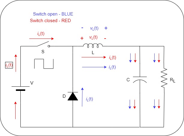
Figure 7 – Block diagram of a buck converter
The voltage at any time across the inductor during this ON period will be in opposition to the battery. Thus, the capacitor and load will see a voltage that is lower than the battery voltage.
When the switch is OFF, the inductor voltage instantly switches direction so as to keep the current flowing in the same direction it had when the switch was ON. The diode D provides a path for this return current.
With proper control of the ON to OFF switching times, a relatively steady voltage lower than the battery voltage can be maintained across the capacitor and load resistor.
The SMPS Controller
Even though almost all SMPS incorporate a chip that takes care of all the control functions, it is still quite instructional to understand how this can be achieved.
Before getting into this, it should be mentioned that a lot of modern SMPS controllers incorporate an internal digital processing block that allows much more sophisticated control loops that enhance the versatility of such controllers.
Figure 8 shows how a simple analog SMPS PWM buck controller can be achieved. It consists of a triangle wave feeding the non-inverting input of a comparator and a sample of the output voltage feeding the inverting input of a comparator.
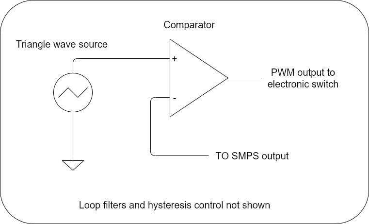
Figure 8 – Simple SMPS analog PWM buck controller implementation
The comparator output will be high anytime the non-inverting input level is higher than that of the inverting input. Note that in an actual implementation, there are loop filter and hysteresis control components to prevent instability in the control loop. These are not shown here.
Figure 9 shows what happens at three different levels of output voltage. When the output voltage is high, the ON time of the PWM output is small. This, of course, causes the output voltage to be brought down.
Conversely, when the output voltage is low, the ON time is larger, causing the output voltage to be higher. Thus, by proper selection of component values, a stable, regulated output voltage can be achieved.
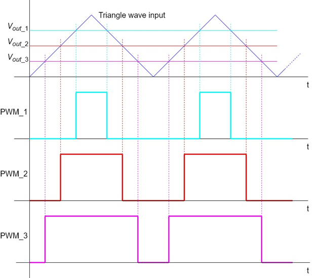
Figure 9 – PWM waveforms at various output voltages
Switching Versus Linear Regulators
There are two kinds of voltage regulators: switching and linear. If the output voltage is higher than the input voltage, then a switching power supply must be used, whether it is a straight boost or some other switching topology.
In the opposite case, a choice can be made between a SMPS or a linear power supply. So, what are some of the considerations?
First is efficiency. Consider, for example, the case of a 1A regulator with an input voltage of 10V, and an output voltage of 5V. Then the power dissipated by the linear regulator (and wasted as heat) will be equal to (10V – 5V)*1A = 5W.
That is a lot of wasted power and most linear regulators will not be able to handle that high amount of power dissipation.
The efficiency in this particular case is at best 50%. This means half of the power is being wasted as heat with only half of the power making it to the output load. It gets even worse if the input voltage is higher than 10V.
On the other hand, a SMPS can achieve 90% efficiency, or more. In this case, it will waste only 0.5W. Even if the energy waste is not a direct concern, you must consider how to safely dissipate this excess heat, especially in confined spaces.
What are the disadvantages of using a SMPS? The first one is cost and complexity. A typical SMPS is more complex, and uses more components, than a linear one. Hence it generally costs more.
Another issue with the SMPS is the presence of ripples on the regulated output. This is simply due to its switching nature. In some cases, this might not be too important. In cases where it does matter, this is generally fixed by having a SMPS followed by a linear post-regulator.
The SMPS brings the input voltage to the point where the input to output voltage differential of the linear post-regulator is suitably small. In turn, the linear regulator provides a cleaner regulated voltage to the load.
Yet another concern is the poor transient response. For instance, it takes a bit of time for a SMPS to react to and compensate for a step or sudden load change. It takes a few cycles of the PWM to properly regulate the output back to where it should be.
Finally, again due to its switching nature, a SMPS does generate unwanted RF interference. So, on top of the additional complexity, more RF suppression components will, in all probability, be needed to get the final product to pass emissions requirements.
Not only that, but in some instances, low-level signal processing blocks must be properly placed, and some consideration should be given to proper PCB trace routing to minimize the effect of this switching noise on these sensitive sections.
Conclusion
This article has provided a brief introduction to switching regulators and some of their characteristics. You should now have a much better fundamental understanding of the operation of switched-mode power supplies.
Hopefully this information will help you select the best power supplies to meet your end product’s power requirements.
Written by Shawn Litingtun

thank you so much for these valuable blogs. I read all of your technical blogs. they’re very helpful in making general views about different topics in hardware design. they’re a lifesaver for beginners like me. please share more about the mechanical aspects.
Thank you!
SMPS can introduce galvanic isolation, unlike the linear supplies.
The size of the SMPS is much smaller comparing to linear counterpart.
SMPS based transformer is also much smaller than the line tranformer in linear supplies.
SMPS are getting cheaper so they will push away linear supplies to be used only for special purposes.
You can buy fabricated SMPS for almost all voltage and power levels. Linear supplies are usually available for special purposes or DIY.
EMC recommendations of switching power supplies would be perfect.