7 Ways to Quickly Judge the Quality of Your Printed Circuit Board (PCB) Design
Are you paying a supposed expert to design your PCB, but you aren’t sure how to judge their work? I’ll teach you how to wisely and safely outsource your PCB design.

In my years of working with hardware entrepreneurs I’ve seen too many cases of poorly designed Printed Circuit Boards (PCB) that would never be of sufficient quality for commercial production.
In some cases these boards were designed by the entrepreneur themselves, and other times they were designed by a freelance engineer.
As I think many electrical engineers will agree, most engineers are never taught PCB design in school, so you need to be careful that you don’t hire an engineer lacking real-world PCB design experience.
Although it really takes an expert in PCB design to do a proper full design review, there are ways to quickly judge the quality of a PCB design.
A schematic may tell you how the individual components are to be connected together to provide a given functionality. However, in and of itself, it offers very limited information about how to actually place, and connect, the components together to provide a functional product.
For example, schematic lines translate to traces on the Printed Circuit Board (PCB). But, the schematic provides little to no information about the kind of signal these lines carry, unless it is explicitly documented in the schematic.
This schematic documentation is especially critical if a different engineer designs the PCB layout than the engineer that designed the schematic.
The signals in those lines could be low-level, low-noise signals that have to be routed away from more noisy PCB traces to avoid noise pickup.
Or, they could be fast data or clock signals that fan out to many pins on multiple chips. In this case, the traces should be matched in length, and be kept short, to avoid mismatched delays.
If such traces are not properly designed, some of the PCB’s might work and some might not, depending on the characteristics and tolerances of the components used to populate each PCB.
In other words, even if a PCB faithfully implements all the component interconnections of a fully working schematic, the end product might not work as intended, if at all.
This article presents 7 ways of quickly judging the quality of your PCB design.
The focus here is on the layout and component placement, rather than the actual quality of the board construction itself (which is solely dependent on the board manufacturer).
Finally, this article is not intended to be highly technical, and certainly does not cover all possibilities, especially for highly complex designs, or designs having unique requirements.
The goal of this article is to show you how to quickly determine if you have a poor PCB design, since there are a few specific areas of PCB design which new designers are most likely to do incorrectly.
#1 – PCB Traces
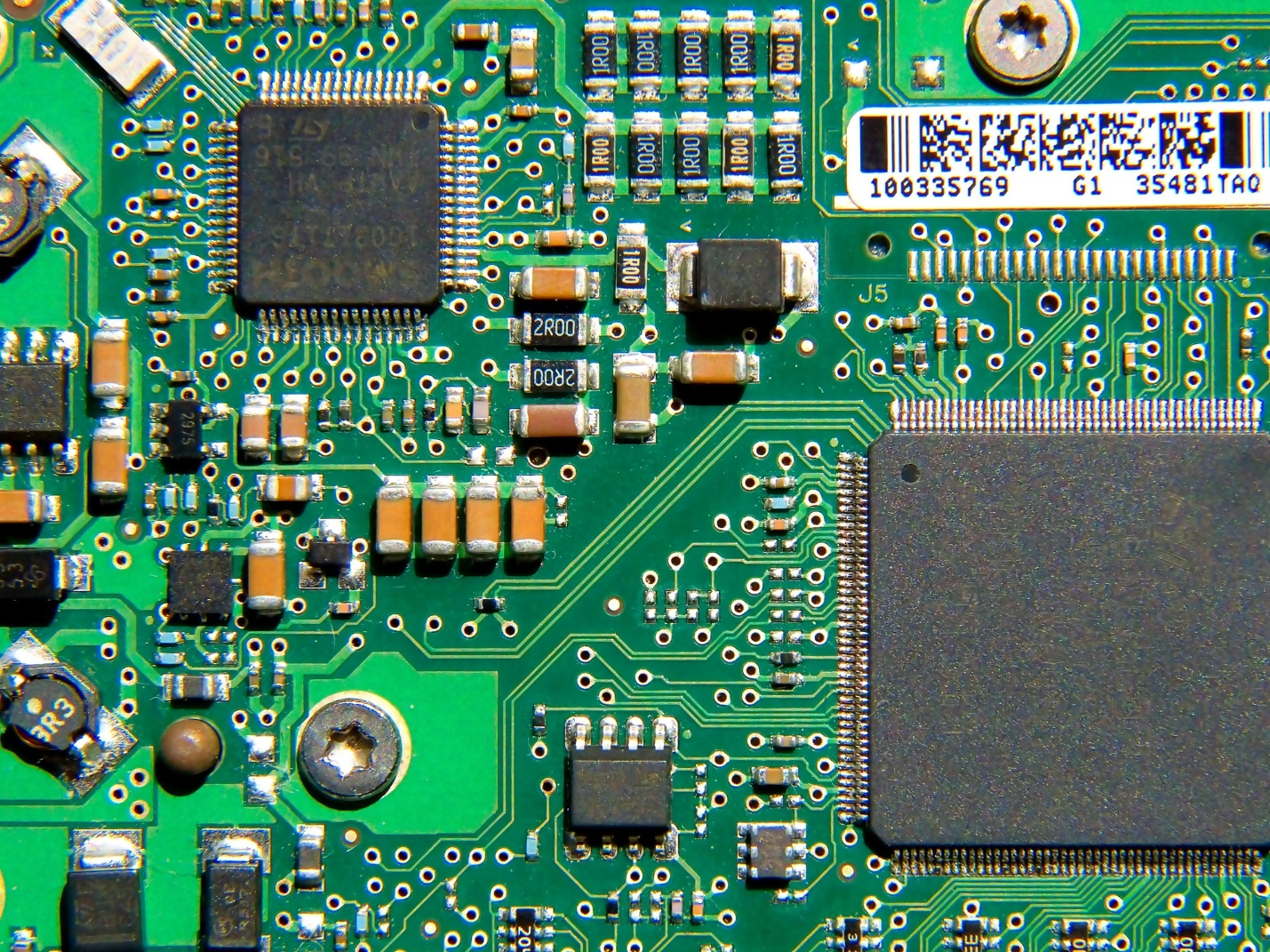
Take an overall look at the visible traces on the PCB. These will be covered by a solder mask, which is a thin lacquer-like layer of polymer that covers the copper traces to prevent oxidation and shorts.
This layer is usually green, but other colors are also available. Note that white solder mask tends to make the traces the most difficult to see. In most cases, just go with the standard green.
Also, only the top and bottom layers are actually visible, and if the board has more than 2 layers you won’t be able to see the internal layers. Still, reviewing the external layers alone should provide some clues as to the quality of the design.
First, look to see if all the traces are running in straight line segments with no sharp bends. Sharp angles can be troublesome for some high power and high frequency traces.
Instead of trying to determine which traces can acceptably have 90° bends, it’s best to simply avoid them. In any case, most CAD PCB layout packages can be set up to avoid this problem.
Note that there are exceptions to this. Some printed inductors are square concentric spirals, and some printed antennas have sharp bends. Both of these, however, are easy to recognize.
#2 – Decoupling Capacitors
All chips need power to function, but what happens when the power source is some distance away from the chip needing the power? In these cases, power has to be brought to the chip via a PCB trace (although typically via a PCB power plane on an inner layer).
Decoupling capacitors are placed very close to the chip’s power pins in order to filter out any high-frequency noise from impacting the chip negatively.
In general, if a chip has more than one VDD pin, then each such pin requires at least one decoupling capacitor, sometimes more.
These decoupling capacitors should be physically placed very close to the pins they are supposed to decouple. If this doesn’t happen, their effect is greatly reduced.
If your PCB design doesn’t have decoupling capacitors placed right next to the power pins on most of the microchips, then that is a big indicator that your design was not done properly.
If you have hired someone to design your PCB and they don’t deal with decoupling capacitors correctly, then you should find a new designer.
#3 – Length Equalization of PCB Traces
The length of the PCB traces must be matched in designs that require a precisely timed relationship between multiple signals. For example, this is critical when routing a high-speed clock signal to multiple chips or the data and address bus lines running between a microprocessor and RAM memory.
This ensures that all the signals arrive at their destinations with the same delays, thus preserving the relationship between the signal edges. This requires access to the schematics, and knowing which set of signal lines require precise timing relationships.
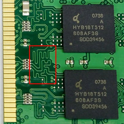
Then, follow the traces to see if some kind of trace length equalization has been implemented (called delay lines). These delay lines will often times look like squiggly lines as shown in figure 1 below.

Note that vias in the signal path cause additional delays. If these cannot be avoided, check that all sets of traces that require a precise timing relationship have the same number of vias. Or, you can use delay lines to compensate for the delays caused by the vias.
#4 – Antenna Feedlines
If your design includes a radio transmitter, receiver, or transceiver (transmitter and receiver combined), then it has to have an antenna.
To achieve the best performance, the feedline between the radio frequency (RF) pin on the RF chip should be impedance matched to the feedline connected to it. This feedline, in turn, must match the impedance of the antenna.
This impedance matching is necessary in order to maximize the power transfer between the antenna and the radio chip.
Any mismatches will cause a decrease in the actual transferred power, and hence a reduced operating range. This feedline is simply a PCB trace with controlled impedance that matches the antenna impedance, which is usually 50Ω.
If the transmitter output impedance does not match the impedance of the feedline then a matching network consisting of inductors and capacitors is usually employed.
In order to achieve a controlled impedance, the feedline is a PCB trace with a calculated width running over a ground plane. The width of this trace depends on the thickness of the copper trace, the thickness and dielectric constant of the PCB substrate.
There are many online tools used to calculate the exact width required for a given copper thickness and substrate material, and it is a good idea to confirm that this indeed is the case in the actual PCB. My favorite is a free software that you can download from Broadcom called AppCad.
If the antenna is a PCB antenna it should be on one edge of the PCB, free and clear of any ground plane. It should be clear of any other traces and away from any large components.
Silkscreen markings around the antenna are usually fine but copper markings, such as a PCB number or company name, can detune the antenna.
#5 – Component Placement
In addition to the placement of decoupling capacitors, there are some other considerations for placing components on the circuit board.
Here are some things to watch out for:
If the circuit contains inductors, they should not be placed too closely together. Inductors create magnetic fields. Placing them close together, and specifically end to end, can cause unwanted coupling between them.
Furthermore, inductors should not be placed close to large metallic objects. The magnetic fields can induce currents in these objects, and this can change the value of the inductors.
Toroidal, or donut-shaped, inductors are usually less prone to have stray magnetic fields, so their effects are less of a concern. If you cannot avoid placing inductors close together, then they should be placed perpendicular to each other to reduce unwanted mutual coupling.
If the board contains power resistors, or any component with significant heat generation, you need to consider the effect of the heat on other nearby components.
For example, if the circuit contains thermistors to compensate for ambient temperature effects, then these should not be placed close to any power resistors. The same applies to temperature compensation capacitors.
If the circuit contains an on-board switching regulator, then all components associated with it should be physically localized to a section of the PCB, and as far away as possible from sections handling small signals. These tend to generate significant switching noise that can negatively affect sensitive circuit sections.
If the PCB has AC mains applied directly to it, usually in the power supply section, then the AC side should be localized to one section of the board.
In addition, the PCB itself should have a physical barrier separating the AC from the rest of the board. Typically, this is accomplished by having a slot in the PCB separating the two sections.
#6 – Trace Width and Routing
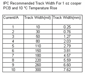
Traces carrying high currents should be sized appropriately. The IPC (Institute for Printed Circuits) recommended trace (also sometimes called a track) width for different current ratings are shown in figure 2 below:
Figure 2 – IPC-recommended trace width for various currents
Traces carrying small analog signals should not run parallel to traces carrying digital or fast changing signals, due to noise pickup issues.
Also, in general, traces connecting inductors should not be any wider than necessary. These can act like antennas, and produce unwanted radio frequency emissions.
#7 – Grounds and Ground Planes
For any moderately complex PCB it is best to use at least a four layer board with the two inner layers being the supply and ground plane.
If the design contains both analog and digital sections, the ground plane should be split, and only joined at a common point, usually the power supply negative. This avoids large ground current spikes from the digital section adversely affecting the analog section.
If using only two layers, then each sub-circuit ground return trace should be separate, and all of them should then join at the power negative terminal.
It is bad design to have the ground return of any sub-section, or IC, join into a common ground return path back to the power supply negative as illustrated in figure 3 below.

The issue here is that PCB copper traces do have some resistance. Thus, current through the trace will cause voltage drops. In the example above, the chip at the far right end of the trace will see its ground reference at a higher voltage than the true ground reference.
What’s more, its ground will bounce around depending on the return currents of all the chips to the left of it in the illustration.
Conclusion
Whether you are learning to design your own PCB, or you plan to outsource it to an electrical engineer, you need to be able to judge the quality of your PCB design.
If you have no design experience and you outsource the PCB design then pay attention to the seven areas highlighted in this article to determine if your engineer is worth what you are paying them.
In fact, if they fail to meet any of these seven criteria then I’d suggest you consider finding a new designer. On the other hand, if you are designing your own PCB, then be sure you avoid these common mistakes.
Regardless though, it’s always a good idea to get a full design review by an independent engineer before proceeding to board prototyping.


This is a unique post. I can’t see posts like this. Where one can discuss the ways to judge the quality of PCB.
Thanks for this worthy tips. about the custome PCB course if it possible, I apperitiated it to creating a video about the final PCB and giving more information about it. I want to know, the above items (specificaly high speed designs) have been addressed?
Some more points I believe to be useful form a designer point of view :-
1.PCB stackup Rules: – Signal layer adjacent to plane and tightly coupled ( 30MHz then Avoid Discontinues plane for return path.
4.Clock signal: – No via, no test points, no multiple signal layer change, clock should couple with reference ground plane, terminate the clock.
5.RF transmission line should be 50Ω impedance control, keep RF trace on top layer with referenced to the ground plane.
6.In MIXED SIGNAL pcb, analog and digital ground planes should be connected via ground plane bridge at a single location.
7.Place TVS diode, MOV near to connectors. Otherwise transients/Surge will couple other signals.
8.PCB Creepage and Clearance should be as per safety standard IEC61010-1, UL60950
9.To avoid GROUND BOUNCE place Decoupling & bypass capacitor close IC power pins. ►Create synchronous designs that will not be affected by momentarily switching pins. ►Add 10-30Ω series resistors at switching outputs to limit the current flow.
Hi Sharad,
These are all great points, thank you for sharing them. The full list of things to check in a PCB design is obviously quite long. I only wanted to quickly touch on a few of the easier ways for anyone to quickly judge the PCB quality. This is why I still recommend a full design review so all of things you mentioned are also checked.
Thanks again for sharing!
Nice post once again, the only thing I found unnecessary is to split ground planes(analog or digital). In some situations yes, but I prefer ground plane to be as much as solid as possible. I often just physically separate analog from digital areas and then just analyze return current paths. Hope this help 🙂
Thank you for the comment and for sharing your experience!