
How to Order Printed Circuit Boards
In this article you will learn about all of the various specifications required to order Printed Circuit Boards.

Ordering Printed Circuit Boards (PCBs) for your product can be rather overwhelming if you’ve never done it before.
If you are outsourcing your electronics design then your engineer will be able to do most of this for you. But if you are planning to do this yourself then you’ll soon discover that there are a lot of complex terms and specifications that you need to understand.
Either way though, as the founder you should at the very least have a basic understanding of the requirements for ordering new boards.
In this article I’m going to break down all of the specifications and terms to help you understand the various tradeoffs.
The specific terms used for some of these specifications will vary from manufacturer to manufacturer, but in general they will apply regardless of where you order your boards.
Basics of Ordering Printed Circuit Boards
Production of a complete PCB consists of two fundamental steps: the fabrication of the empty board itself, and then the soldering (assembly) of all of the components. This articles separates all of the various specifications into these two fundamental steps.
When ordering the PCB fabrication (empty boards) you will need to supply the manufacturer with what are called Gerber files which are generated from your PCB design software.
For the PCB assembly you will need to supply them with a Bill of Materials (BOM) listing all of the components, as well as what is called a Pick-and-Place file that contains the precise locations of each component that will be used for programming their automated soldering equipment. Both of these files are also generated by your PCB design software.
PCB Fabrication
Standard Specifications
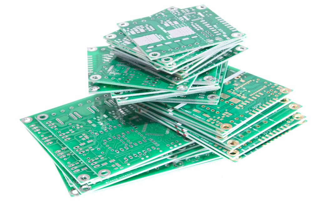
Board type: In most cases you will select “single pieces”. Printed circuit boards are not manufactured individually. Instead they are produced in larger panels containing multiple copies of your board. This allows more efficient production for smaller boards.
After PCB assembly (soldering of components) or perhaps after final testing is completed the individual boards on each panel are then separated or depaneled.
In most cases you will not need to worry about panelization and the manufacturer will supply you fully assembled boards that have already been separated.
Different Design in Panel: It is possible to have different boards combined together on the same panel. If your product requires multiple different boards then you can have them all on the same panel to save costs. Although there is an additional fee for having a panel with different board designs.
Size: If ordering single pieces then this is the dimensions of your individual board which is a critical factor in the PCB cost. If ordering panels this is the panel dimensions.
Quantity (single): Start with 5 boards on your first version, then slowly increase as your confidence in the design improves.
Layers: This is the number of routing layers used in your PCB design. Except for a single layer it is always an even number. The simplest PCB uses 1-2 layers (top and bottom). Most moderate complexity designs (i.e. microcontrollers) require 4-6 layers, and more complex designs (i.e. microprocessors) requires 8 or more layers. The number of layers directly impacts the cost of the PCB.
Material: The is the base material used in the PCB between stacked routing layers. FR-4 is by far the most common material which is sufficient for most designs.
FR-4 comes in different Tg versions where Tg is known as the glass transition temperature. It is the temperature at which the material begins to lose its rigidness and becomes more rubbery. For most designs TG150-160 is a good choice with no additional cost. Stepping up to TG170-180 adds considerable cost.
If your design has custom RF circuitry (including antenna feedlines) then a RF specialized base material may be needed. Rogers R4000 series of materials are the most commonly used material for RF designs. R4003C is a halogen-free material which is more environmentally friendly than R4350B. Both have fairly similar RF related specifications.
If your design is high power then a base material with a metal core may be necessary for improved power dissipation. This is especially common in high power LED lighting applications.
An HDI (High Density Interconnector) board is one with a higher routing density, smaller features, and a high layer count than a standard PCB. This process is usually reserved for very complex designs, or exceptionally small designs, and the cost will be many times higher than for a standard PCB.
Blind vias and buried vias are only used when small size is critical because they significantly increase the board cost. Normal vias are through-hole meaning then go through all layers, even the layers where they are not needed. These vias can take up unnecessary space on the layers where they are not connected. A blind via connects from an outer layer to an inner layer so you can only see one end visibly on the final board. A buried via instead connects between two inner layers and is totally invisible on the final board.
Thickness: This is the final thickness of the board. The most common thickness is 1.6mm ( 0.062”). If space or weight are critical then you will select a thinner board. If strength of the board is critical then a thicker board will be best.
Min track / Spacing: This is minimum allowable width for any routing traces/tracks and the minimum space allowed between traces. This is measured in mils (a mil is a thousandth of an inch). 6 mils is probably the most common, but many designs where space is critical may need to go down to 3 to 5 mils. Once you go below 6 mils the price begins to increase significantly.
Min hole size: This is the minimum hole size that can be drilled. This is mainly the hole for use in vias which connect traces on different layers. Vias can take up considerable space so a smaller hole size will allow a tighter packing of the components.
Solder mask: Solder mask is protective layer that is added to the outer layers of the board to prevent oxidation and solder bridges (shorts) between adjacent solder pads. Green is by far the most common color, but you can also select for other colors.
Silkscreen: Silkscreen is a layer for adding text and simple images (logo) to your board. It most commonly adds the component identifiers.
Gold fingers: If your board has edge connectors then you will want those to be gold plated for corrosion and abrasion resistance.
Surface finish: The surface finish is a coating added to exposed copper pads on the outer layers of the board to prevent corrosion and improve solderability. In the past HASL was the dominate choice but it has mostly been replaced by ENIG (Immersion Gold) because it is lead-free. Immersion silver (Ag) is also a lead-free finishing option.
Via Process: Normally vias are left open but there are times you will want them to be closed. The simplest and cheapest option (actually there is no additional cost) is tenting the via which simply means letting it be covered up by the solder mask layer. Tenting mainly works with smaller diameter vias.
A more expensive process is to actually fill or plug the vias. This is commonly used on tight spaced BGA packages where you need to place vias very close to the chip pins. These vias can wick away solder from the chip pin leaving a poor quality solder connection. Plugging the vias in this case can solve this issue.
Finished copper weight: This is the weight of the copper layer spread out over 1 square foot. It really is a measure of the copper thickness. For example, 1oz of copper equivalates to 1.4 mils of copper thickness. Thicker copper traces are primary used for high power designs so as to require less wide traces to carry the same amount of current. This is for the outer routing layers.
Inner copper weight: This is the copper weight (see Finished copper weight above) for the inner routing layers. In most cases it’s best to route high current traces on the outer layers for better heat dissipation.
Additional Options
Peelable solder mask: This is a coating layer used to protect areas of the board (such as edge connector pins) during the assembly process. After assembly is complete you can then peel away this coating which only served to provide protection during the board assembly process.
UL Marking: PCB’s are flame-retardant and are UL94V-0 certified. You have the option of having this certification mark stamped on the board.
Half-cut/Castellated Holes: Castellated holes are commonly used on PCB modules which are designed to be soldered onto another PCB board.
Halogen-Free: Less than 1,500 ppm for total halogens.
Via in pad/ Via filled with resin: Normally vias are not permitted inside of solder pads because the via hole acts to wick away solder thus potentially leaving a bad solder connection. However, in some cases such as with high pin count BGA packages with a small pin-to-pin pitch, the limited space requires the use of vias in the pads. Some chip manufacturers will also specify vias in a pad to improve the heat transfer properties.
Z-axis milling: A variable level elevation can be milled at the edge or within a circuit board.
Edge Plating: This is copper plating that runs along at least one edge of the board.
Custom Stackup: The stackup is the order in which the various board routing layers are stacked.
Press-fit holes: Contact holes where a lead is press fitted in instead of soldered.
Impedance control: Impedance control is necessary for some more complex high-frequency digital or analog designs. It consists of measuring the impedance of certain traces when the PCB is manufactured to make sure they are withing the design limits for proper signal propagation. It adds considerable cost so it is only used when absolutely necessary. It is not necessary for most designs.
Carbon mask: Carbon ink is used to create surface resistors and a protective contact surface for switches.
Countersinks/Counterbores: These are drilling methods that allow a fastener (such as a screw or bolt) to sit flush with the top surface of the board.
PCB Assembly
Standard Specifications
Component sourcing options: Turnkey or Kitted or a Combo. Turnkey means they will source and supply all of the components, kitted means you will supply the components, and then combo is just a combination of these two options.
Board type: This sets whether the boards are assembled as single pieces, or if they are assembled as a panel. For board counts higher than 20 pieces or board sizes smaller than 50mm per side then panelized will be preferred so as to make the manufacturing process more efficient.
Quantity: The number of individual PCBs to be assembled.
Number of Unique Parts: This is the number of unique components that will need to be soldered onto your board. For example, if your design uses five identical capacitors in various places that would count as one unique component. This count includes every unique chip, resistor, capacitor, inductor, connector, etc.
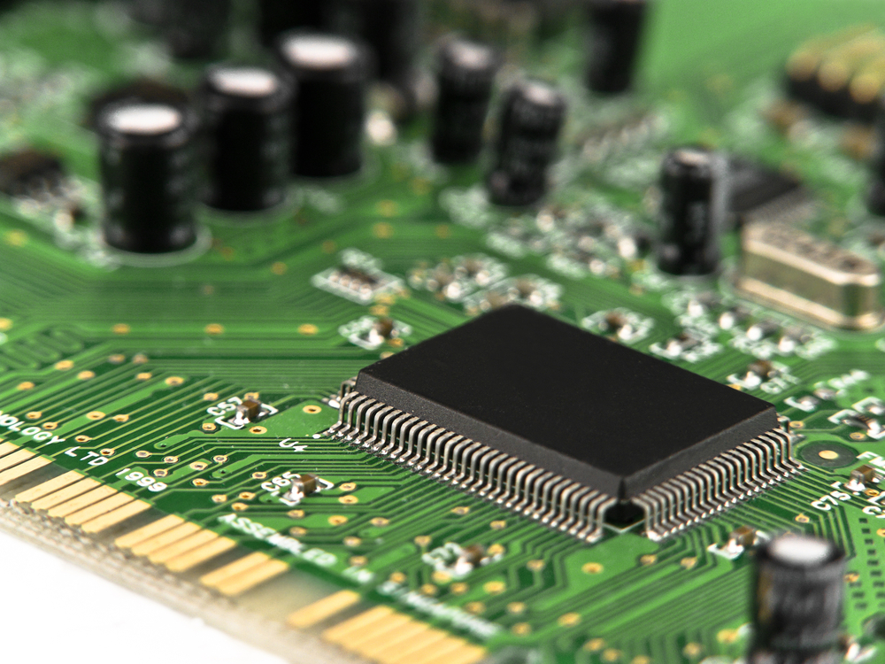
Number of SMT Parts: This is the number of components that require Surface-Mount Technology (SMT). This number counts all of the components and not just unique ones. For example, if you have five identical SMT capacitors that would count as five SMT parts.
Number of Through-Hole Parts: This is the number of components that require a through-hole assembly process. Through-hole parts are rarely used on modern electronic designs except in cases where a higher strength attachment is necessary such as for a connector that will experience regular forces.
Additional Options
Depanel the boards: If the assembly process is done on panelized boards then you have the option to have the individual boards separated before shipping to you.
Conformal coating: This is a protective layer placed over the assembled board that conforms to the topography of the board components. It is used to protect the electronics when used in harsh environments or high humidity.
Press-fit connectors assembly: As explained above for the PCB fabrication a press-fit connection is one that does not use solder. The electrical connection is made by pressing a lead into a matching hold that forms a s good electrical connection. These are not common.
Function test: This is done to confirm the board has good solder connections, the correct components were installed, there are no shorts or open circuits, etc. You will need to provide testing details to them.
Firmware loading: If your PCB includes a microcontroller you can either load the firmware yourself or have them do it for you. During development you will need to do this yourself, but once in production then I suggest you have them upload the firmware.
Number of X-ray test: For designs using packages with hidden leads underneath the part such as BGA parts it is not possible to perform any visual inspection since the solder connection is hidden under the part. This is when X-ray inspection is needed.
Conclusion
When it comes to ordering professionally produced boards, whether that be low quantities for prototyping, or higher volumes for production some of my favorite manufacturers include Seeed Studio, PCB Way, and Bittele in China, and in the U.S. I recommend Sunstone Circuits.
Although you do have the option of assembling your own boards by hand, in most cases I don’t recommend it unless you are very skilled at soldering. Most modern microchips are simply not feasible to hand solder.
Also one big downside with hand soldering is if you find problems with your design it can be challenging to differentiate between bad soldering and more fundamental design issues. By ordering boards and assembly from a professional manufacturer it will greatly simplify the testing and debug of your design.
Although there are a lot of technical terms that you must know to order printed circuit boards, hopefully this article has helped you to better understand those requirements.

Nice article, but don’t scare folks away from hand soldering prototypes, it’s not hard at all, even with dense packages and modern chips. As long as they aren’t doing BGA it’s totally feasible to hand solder. Maybe that should be another article!
Thanks for the feedback. I guess I just hate soldering and even though I’ve been doing it since I was a kid I never got great at it. I always just have preferred getting boards professionally assembled so I don’t have to worry as much about soldering issues causing problems.