
Introduction to Analog to Digital Converters (ADC)
There are many different implementations of an Analog to Digital Converter, or ADC. This article provides an overview of the main types, their characteristics and limitations.

Almost all microcontrollers have built-in ADC’s. Even the small Arduinos, based on the AVR ATMega family, have them. The last section of this article deals with some of the issues to be aware of when using such ADCs. But first we’ll review the basics of Analog-to-Digital conversion.
Basics of Analog to Digital Conversion
An ADC is represented by the schematic symbol in figure 1. It just shows an analog input, and its equivalent digital output. The example shown is an N-bit ADC. N is typically anything from 6 to 24, with common ones being 8, 10, 12 or 16.
The input is a voltage, with a range of 0 up to some maximum value that depends on the actual ADC. Given that with N-bits there can be 2N possible digital values, then the value represented by one bit is (VADCMAX / 2N).
As an example, if the maximum input value of a given ADC is 5.0V, and the ADC is a 10-bit type, then each bit represents (5V / 210), 5.00 /1024, or approximately 4.89mV. So, this particular ADC has a resolution, or quantization step, of 4.89mV. This is its absolute theoretical resolution.
In this particular case, a signal cannot be resolved to a resolution better than ± (4.89mV/2). This limit is called the quantization error, and all ADCs, even perfect ADCs, have quantization errors to a given extent, depending on the resolution of the ADC.
Practical ADCs have even more sources of error. Two such errors are: Differential Non-Linearity, or DNL, and Integral Non-Linearity, or INL, errors. These have to be taken into account when specifying an ADC for a particular application.
DNL errors occur when the ADC output does not change when it should have. For example, assume that the current output code is 01101100 for a given input, and that the input value increases by half a quantization step. The code should then be 01101100 + 1 bit, or 01101101.
The reverse can also occur when the input voltage is lower than the current input voltage. Sometimes, this doesn’t happen for various reasons. The ADC, in this case, is said to have a ±1 bit DNL error.
INL errors occur if the quantization levels are not evenly distributed throughout the entire input range. For example, say a particular ADC has 12 bits, or 4096 counts, of resolution and a 4.096V reference voltage. Each bit count represents exactly 1.000mV of input voltage change.
So, an input voltage of 4096 mV should give an output of 1111 1111 1111, or 0xFFF. For some ADCs, an input of 4095mV, or even 4094mV, would still give a digital output of 0xFFF. What happened is that over the entire input range, value of 1-bit changed ever so slightly to say, 1.001mV, or 0.999mV. The accumulated error resulted in a full-scale error of one or two bits of accuracy.
As will be seen later, there are many external factors that will degrade the ADC output accuracy even more.
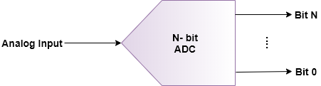
Figure 1- Schematic representation of an ADC
ADC Implementation
There are many ways of implementing an ADC. The next few sections present several of the more common ones. To keep this article relatively short, only simple and somewhat incomplete descriptions of each such implementation are given.
Single and double slope Integration ADC
The block diagram of a single-slope ADC is shown in figure 2. Basic operation is very simple. A capacitor is charged from the input source until its voltage reaches VRef, at which point the comparator trips. While charging, a digital counter fed by a clock was also counting. It stops counting when the comparator trips, at which point the count reached is a representation of the analog input.
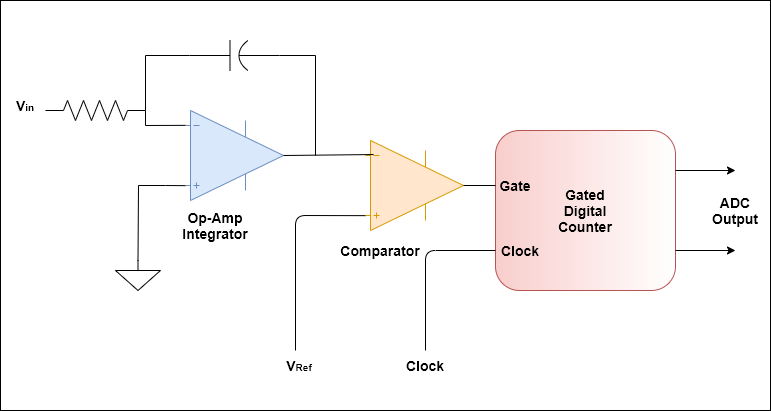 Figure 2 – Block diagram of a single-slope integration ADC
One of the most common variations of this method is the dual-slope integration ADC. In it, the capacitor is then discharged, and the counter value is averaged. This technique mitigates the effect of dielectric absorption, an effect that can cause errors in the ADC reading, in the integrating capacitor.
This type of ADC is accurate, but very slow; it is mostly used in multimeters, for example, where accuracy is more important than speed.
Sigma-Delta Σ-∆ ADC
The Sigma-Delta, or Σ-∆, ADC block diagram is shown in figure 3. Starting with the input side, the difference amplifier produces an output that is the difference between Vin and the DAC output.
The 1-bit DAC has an output that can be at one of two values: -VRef or +VRef. The integrator in this case can best be thought of as taking the moving average of the previous value and the current input value.
So, to start, assume Vin is fixed at just a very tiny bit above 0V so that the comparator will trip. Its value will be high, or 1. The DAC output will then be +VRef. On the next round this value will be subtracted from the current value of Vin. The integrator output will now be at – Vref since the previous value was 0V. The comparator output will now be 0, and the DAC output will be at – VRef.
On the next sample, the integrator output will be 0 since the previous value was at – VRef, and the difference amplifier actually subtracted -VRef, and thus added, VRef to Vin. The comparator output will thus be 1.
This process continues, and the comparator output will thus be a steady stream of 101010… for a Vin of 0V. Remembering that logic 1 means VRef, and 0 means -VRef, then if N number of samples are taken and averaged, it is easy to see that the average will be 0V. The processing block after the comparator will simply output this as a single value of 0000… assuming a reference of (VRef – -VRef), or 2 x VRef.
Now, assume that Vin is 1V, and this is a 5V ADC; ±VRef is ±2.5V. Working out the same steps as before, the output will be: 1011101… This works out to be 1.07V.
However, if more samples are taken the precision becomes greater, and the value gets closer to 1.00V. Thus, the Sigma-Delta requires many samples in order to generate one output. In other words, the input signal needs to be over-sampled to reduce the ADC conversion errors.
Sigma-Delta ADCs are typically used for digitizing audio signals, and as the ADC in some microcontrollers.
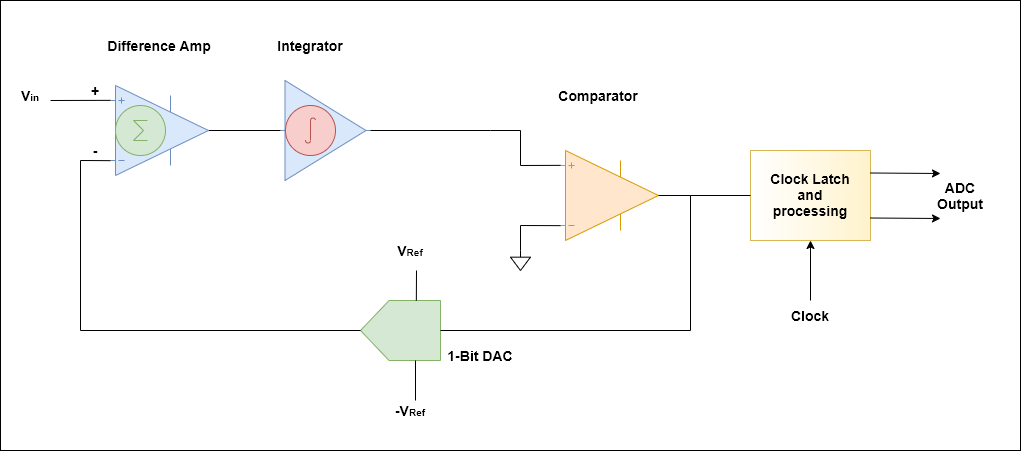 Figure 3 – Block diagram of a Sigma-Delta ADC
Flash ADC
The operation of a flash ADC is perhaps the easiest to understand. Figure 4 shows the block diagram of a flash ADC. It is just a lot of comparators each fed with a reference voltage that is one bit-value higher than the previous one. So, for an 8-bit ADC, 256 such comparators are needed; for a 10-bit one, 1024 are needed.
The flash converter is fast. It directly converts the input without any kind of sampling or heavy post processing. The issue is that it requires a lot of comparators, and that many comparators take up a lot of silicon real estate on a chip. So, the flash ADC is only employed when extremely high speed not attainable by other ADC implementation methods is needed.
What has just been described is actually known as a full flash ADC. One commonly used variant is the half-flash ADC. It uses a two-step process to cut in half the number of converters required in the actual conversion chain.
First the input signal is compared to a level set exactly at half VRef. If it is lower, then the most significant bit, MSb, is set to 0, and the input is fed to a comparator chain with a reference voltage set to VRef/2 to actually get the remaining bits.
If the input signal is higher than VRef/2, the MSb is set to 1, VRef/2 is subtracted from the input signal. This can be done, for example, by offsetting the lower end of the reference resistors by +VRef/2.
The comparator chain is again used to get the remaining bits. So, essentially this uses half the number of comparators of a full flash at the expense of one additional comparison. This technique can also be extended to have quarter flash ADCs, for example.
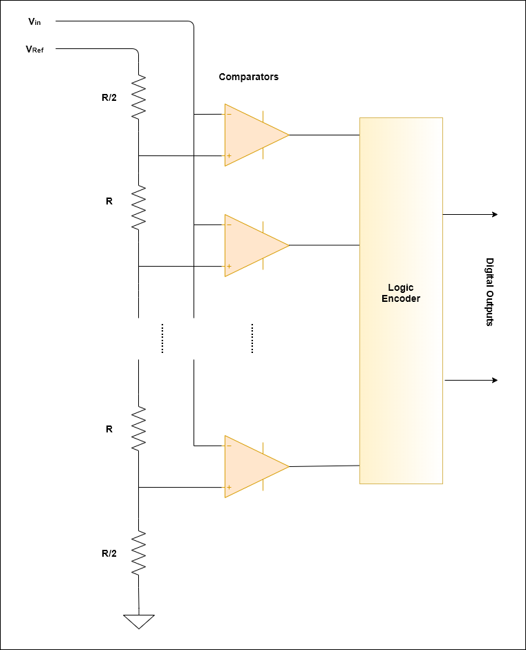 Figure 4 – Full flash ADC
Successive Approximation Register (SAR)
This is the ADC technique that is most often used in medium speed ADC’s. The block diagram of a SAR ADC is shown in figure 5. The SAR operation is the key to this ADC. Initially, it is set to the mid-point of the DAC range.
The comparator output will either be high or low, depending on whether the input was higher, or lower, than the DAC output level.
Now, the input is either in the upper half or lower half of the DAC range. The DAC is now set to the mid-point of the DAC upper, or lower, half of the correct range where the input lies, effectively reducing this range to one quarter of the entire range.
This process is repeated, successively narrowing the range where the input lies, until it has zoomed in to the correct value.
Another way of looking at this is to say that after the first iteration, the MSbit of the input will be known, and it is either 0 or 1 depending on whether the comparator output was low or high. After the next iteration, the next MSbit will be known. The process is repeated until all the output bits are known.
One thing that was not mentioned is the Track and Hold, or T&H, block. The iterative process will be disrupted if the input value were to change during the ADC conversion process. The T&H block simply captures the input value at the start of the conversion, and holds this value during the entire conversion.
This is illustrated in figure 6. The T&H output keeps the value of the input signal at the point where it was triggered regardless of what the input signal does afterward. After the conversion is complete, the T&H will again go back to tracking the input signal.
The SAR ADC is the most widely used ADC, and is the one found in the built-in ADCs of most microcontrollers. Some use Sigma-Delta ADCs, but most have SAR ADCs.
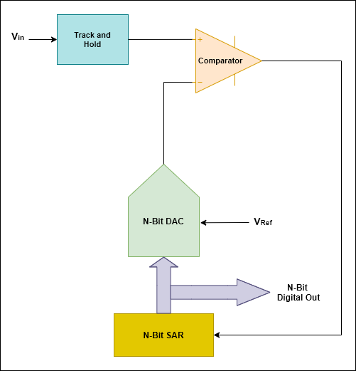 Figure 5 – Block diagram of a SAR ADC
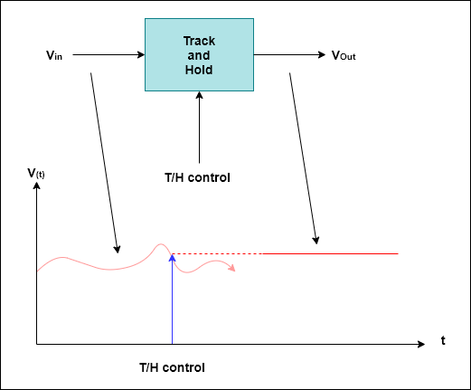 Figure 6 – T&H block diagram
Microcontroller ADCs
Almost all microcontrollers have built-in ADCs, most with multiplexed inputs. To be effectively used, their limitations should be taken into account.
First of all, based on what has been covered so far, it should be obvious that the input cannot have a range that exceeds the ADC VRef, and the conversion rate limits of the ADC have to be observed.
For example, the maximum ADC conversion rate of an Arduino Uno is less than 10KHz. So, there is simply no way to sample full audio of 20Hz to 20KHz bandwidth with this ADC.
The issues with microcontroller-based ADCs all boil down to the fact that microcontrollers are CMOS devices, and the silicon process used to manufacture microcontrollers is not quite compatible with implementing analog circuit blocks.
So, the DACs and comparators, for example, do not use precision resistors because these are really hard to implement in a CMOS silicon process. Instead, they employ a functionally equivalent design that uses capacitors. The net result is that the ADC input of the microcontroller has a relatively low impedance that is also capacitive.
What’s more is that the input impedance changes somewhat during a conversion process. This all means that if the output impedance of the source is high, then the ADC is prone to give conversion results that are way off. Figure 7 illustrates this point with an example.
In this example, the ADC is used to read the 6-V battery voltage. In order not to overly discharge the battery, R1 and R2 are chosen to be both 20KΩ so that the ADC input is 3.0V when the battery voltage is 6V. The ADC has a VRef of 3.3V; so, everything should work fine.
However, a typical microcontroller ADC has an input impedance of about 10KΩ, and as seen, it is in parallel with R2. This will cause a very large error in the battery voltage reading. The solution in this case, would be to have an external buffer driving the ADC input.
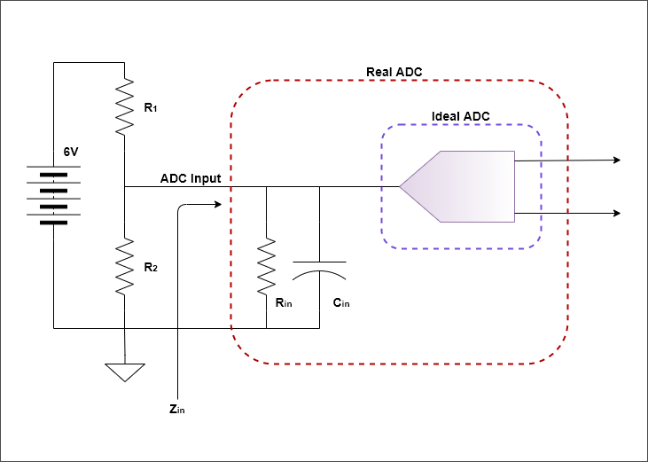 Figure 7 – Illustration of the effect of ADC input impedance
One last thing that should be considered when using microcontroller ADCs is the ADC reference. In some microcontrollers, this is simply the microcontroller VDD.
For sure, the microcontroller VDD is derived from a voltage regulator, but there is a big difference between a voltage regulator and a proper voltage reference.
This can easily cause at least two bits of accuracy loss. Because of this, the 12-bit microcontroller ADC is now more like a 10-bit ADC, and that’s not counting DNL and INL error contributions.
Bottom line is be aware of these limitations, and determine if the microcontroller ADC is suitable for the application.

This is much clearer than the data books ever were. Thanks John!
An N-bit ADC has bits 0 thru N-1 (Not N).
E.g. a four-bit ADC returns bits 0 thru 3.