
Introduction to Load Cell Conditioning Circuits
A load cell is a sensor device that can be used to measure an applied physical force and then convert that force into an output quantity that is directly proportional to the force.

Article Technical Rating: 6 out of 10
There are different types of load cells such as hydraulic load cells, pneumatic load cells, capacitive load cells, strain gauge load cells, etc. The most popular and commonly used of all these types is the strain gauge load cell.
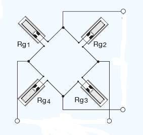
Figure 1: Load cell Wheatstone bridge circuit
A strain gauge load cell produces an electrical voltage signal that is proportional to the force applied. This output signal, however, is very small in magnitude. Most load cell circuits are setup in a Wheatstone bridge configuration which is a simple circuit commonly used to measure an unknown resistance.
The sensitivity of a strain gauge is rated in mV/V meaning the maximum output is a function of the excitation voltage. For example, with a gauge sensitivity of 10mV/V and an excitation voltage of 5V, then the maximum output voltage is 50 mV in magnitude.
This small signal, therefore, needs to be conditioned before being fed to an analog-to-digital converter (ADC). Signal conditioning involves filtering and amplifying the signal.
Amplifiers
Amplifiers are electronic devices built from components designed to amplify the load cell’s small output signal (in mV) in the presence of large common-mode voltage signals. There are basically two different types of amplifiers that can be used for this purpose, which are the Operational amplifiers and the instrumentation amplifiers.
An operational amplifier, also called an op-amp, is one of the most crucial components of any analog electronic circuitry. They are extensively used in signal conditioning systems for amplification, filtering and also for performing some mathematical operations.
The diagram below shows the circuit model of an ideal op-amp.
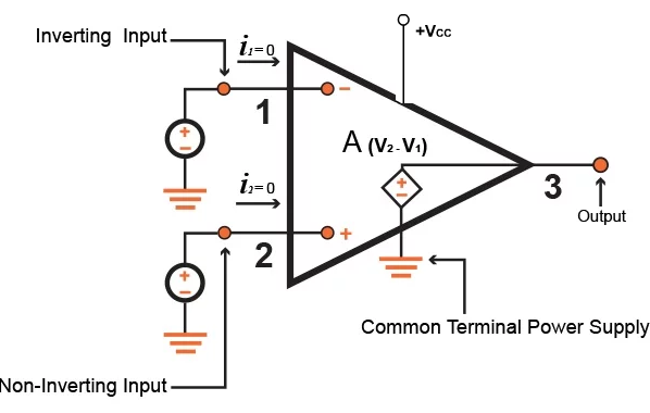
Figure 2: Ideal op-amp without feedback
Its operation can be explained as follows; the op-amp is designed to produce an output which is the amplified difference between the voltage at the inverting input and the non-inverting input. This can be expressed mathematically as:
Vo = Av (V2 – V1)
Where Vo is the output voltage, Av is the op-amp gain, V1 is the inverting input, and V2 is the non-inverting input.
Furthermore, it can be seen that the input current at each input pin is Zero. Therefore, the op-amp does not draw in any current, and hence the input impedance is infinite. Since no current is ideally entering the op-amp, the output current is sourced from the power rails as shown in the model circuit above.
It should be noted that in practical terms, an infinite impedance simply means the input impedance is very high.
In most cases op-amps are used in a closed loop configuration. This means that a portion of the output is fed back to the input allowing you to set an accurate gain.
The most efficient type of amplifier to use for the load cell’s output signal is the instrumentation amplifier due to its large common-mode rejection ratio, high open-loop gain, low noise, low drift, very low DC-offset and very high input impedances.
The diagram below shows the basic circuitry of an instrumentation amplifier
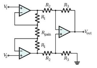
Figure 3: Basic setup of an instrumentation amplifier
From the diagram above, it can be seen that an instrumentation amplifier is made from a special connection between three operational amplifiers.
This instrumentation amplifier allows for its closed loop gain to be adjusted without changing more than one resistor value in its circuit. The gain is expressed mathematically as shown below:
(1 + 2R1/Rgain) x R3/R2
Furthermore, in most commercial load cell conditioning devices, the amplifier is also setup to have a programmable feature which allows its gain value to be set by a computer program. However, the gain values that can be obtained are limited to a set of values, which are usually about two values.
Electronic Filtering
Filtering is the process that removes undesirable electrical noise that may interfere with the load cell output signal. This electrical noise may be electromagnetic interference from neighboring equipment or other component parts, especially when the load cell output signal is routed through a printed circuit board. These noises appear as unwanted signals at undesirable frequencies, so they behave like AC signals.
There are different classes, categories, and types of filters However, filters basically can be:
Low pass filter – Pass low frequencies, reject high frequencies
High pass filter – Pass high frequencies, reject low frequencies
Bandpass filter – Pass a narrowband of frequencies
Band-rejection filter – Reject a narrowband of frequencies
The type of filter used in the design of a load cell circuitry is a low pass filter. A low pass filter is designed to allow the low-frequency signal from the load cell to pass while rejecting the high frequency noise.

Figure 4: Simple low-pass RC filter
A simple low pass filter can be created with just a single resistor and capacitor as shown above. More advanced filters may include an inductor, or even op-amps to provide active filtering.
The above RC filter acts as a low-pass filter primarily because of the behavior of a capacitor. The impedance of a capacitor decreases as the frequency increases. So to a high-frequency signal a capacitor can appear like a short to ground. Therefore, all of the high-frequencies are passed into the ground instead of the output.
To low frequencies the capacitor appears as a high-impedance, or an open circuit, so low frequencies are passed to the output.
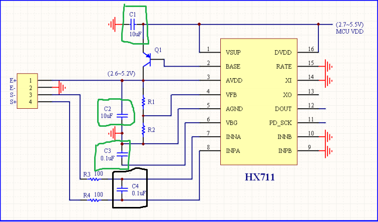
Figure 5: Reference circuit for the HX711 (a common load cell amplifier IC)
Referring to figure 5 above for the commonly used HX711 load cell amplifier, the filtering capacitor is placed in between the two wires carrying the output signal. The filtering capacitor is highlighted in the color black between the two signal lines S- and S+.
This capacitor coupled with the two 100 resistors forms a differential RC low-pass filter. To a high-frequency noise signal both inputs appear shorted together so there is no differential signal.
Note that the capacitors highlighted in green are decoupling capacitors. These capacitors help to provide a stable power supply free of interfering electrical noise.
Conclusion
In conclusion, it can be said that signal conditioning involves techniques used to enhance the quality of the sensors output signals. It has the following functions:
1) It protects the other components of the overall system by controlling the output current/voltage signals.
2) It transforms the sensors output signal into a voltage/current level which can be processed by other digital components of the system.
3) It also helps to attenuate/filter off ground noises or other electrical noise from neighboring equipment.
This article is a guest post by Joe Flanagan. Joe has over 15 years experience with sensors and data acquisition. He is currently a Project Engineer at Tacuna Systems (the load cell specialists).
