
Introduction to PCB Assembly Manufacturing
In this article you will learn how Printed Circuit Boards (PCBs) incorporating Surface-Mount Technology (SMT) components are assembled in a production environment.
This article is written by the team at NeuronicWorks, which is a product design, prototyping and manufacturing organization based in Toronto, Canada catering to various industries.
With miniaturization of electronics and the need for smarter, accessible, and precise technology, surface mount technology (SMT) became the technique of choice for Printed Circuit Board Assembly (PCBA) in the early 1980s.
Before the popularity of Surface Mount Technology, through-hole technology was the order of the day where component leads (axial or radial style) are inserted through holes on a bare PCB and then soldered.
While one side of the board was called the “component side”, the other was called the “solder side”, terminology that is still in use today.
Even today, both technologies are still in use and can coexist even on the same board, both offering their own set of advantages.
As through-hole technology results in stronger physical connections, it is considered a better approach to design high-reliability products for rugged or even commercial applications that can withstand environmental stress.
It is also a great option for components that may undergo mechanical stress (i.e., vibrations) due to their mass such as connectors or for larger components like decoupling capacitors, transformers, etc.
Surface Mount Technology, originally termed as planar mounting, is a method where electrical components are mounted onto the surface of a printed circuit board with flat-formed leads or small metal pads.
This technique is helpful when PCBs are required in high volume or with a need for miniaturization to meet unique requirements.
Unlike through-hole technology, surface mount allows for conveniently mounting components on both sides of a board within limits as the SMT technology requires vias to create connection in between board layers.
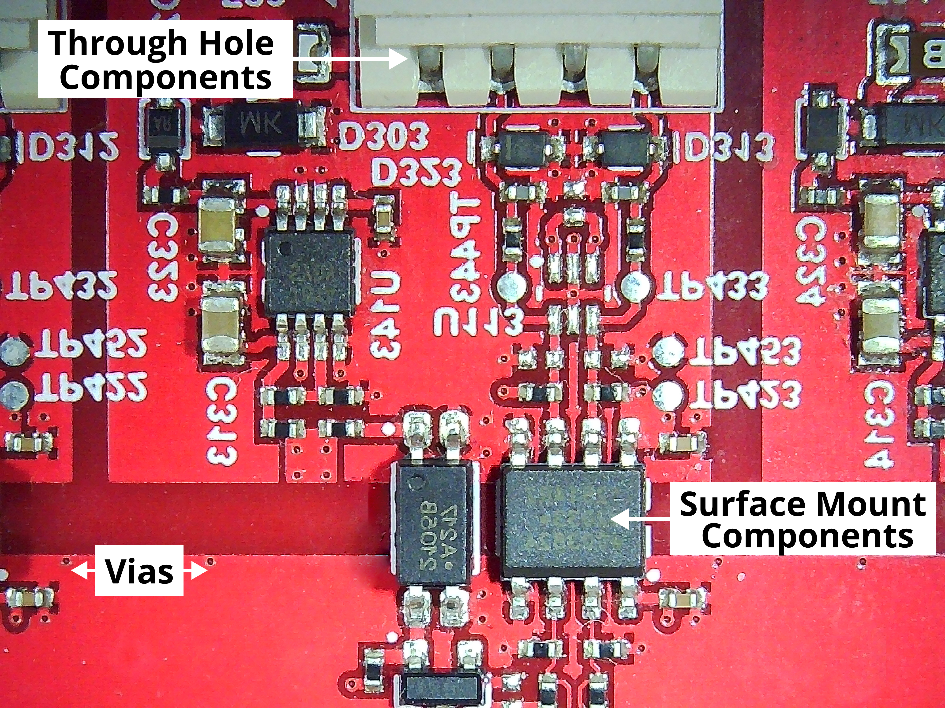
Fig 1: Board with Through Hole component, Surface mount components and vias
Multilayer SMT PCB stackups today range from having 2 layers to 32 layers, with the most common ones using 4 and 6 layers.
Surface mount technology has been advantageous in this case by further reducing the size of PCBs by increasing the number of connections per square inch of PCB.
For a better understanding of the level of complexities, let’s look at the inside of a PCB stackup.
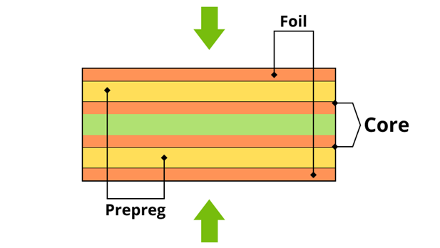
Fig 2: PCB stackup
Notice in Fig 2 that the PCB is made up of several layers. This arrangement of materials is referred to as the “PCB stackup” and can vary depending on the PCB requirements.
The two key components of a stackup are the copper foil layers – for conducting electricity – and the laminate layers – to provide structure and insulation.
Copper foil layers are “etched” to draw specific wiring patterns and can vary in thickness: thicker layers allow for more electrical current to flow.
The standard copper thickness used is 1 oz. Interestingly, copper thickness in PCB production is measured in ounces (oz.) where a specific weight of copper is rolled out to occupy 1 square foot (equals 1.37 mils or 0.0348 mm).
Additionally, 1.5 oz and 2 oz are also standard copper thicknesses which will allow proportionally higher currents to flow within the circuit.
Laminate layers are composed of fiber-reinforced epoxy. They come in two basic flavors: “Cores,” that have copper foil pre-cured to them, and “PrePreg,” without copper foil, in which the epoxy is not fully cured.
When the stackup is assembled and cured by pressure and heat, the PrePreg layers act as a glue that holds all the layers together.
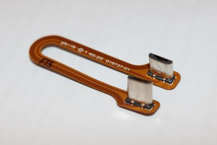
Fig 3: Flex PCB
The most common type of laminate used in PCB manufacturing is called “FR4,” but different laminates (BT Epoxy, Polyimide, Teflon, etc.) can be used for more demanding applications, such as high-frequencies or high-temperatures.
At the same time, there are different types of PCBs: Rigid, Flex and Rigid-Flex. Rigid PCBs are the more conventional PCBs which true to its name are rigid or inflexible in nature.
Flex PCBs are built by replacing the core, or prepreg layers, with thin polyimide layers, which can be bent or shaped to suit space constraint requirements.
Flex PCBs are becoming more mainstream today due to miniaturization and popularity of wearables.
Rigid-Flex on the other hand is a combination of both rigid and flex PCBs, combining the versatility of flexible circuits with the stability of rigid PCBs.
The reliability of the inter board connection is increased by eliminating the need for connectors and cables, which is a more reliable system.
It is the most expensive type of PCBs and is used mostly in aerospace or military applications.
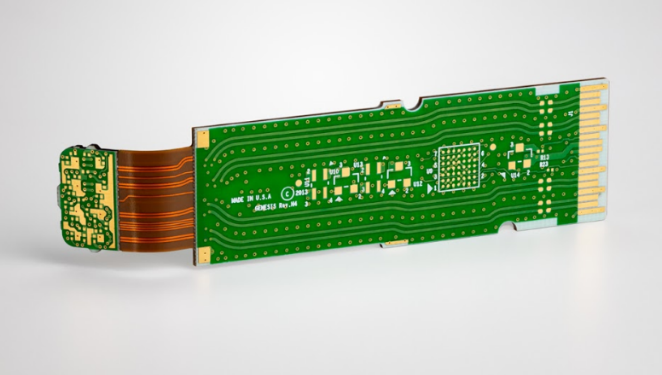
Fig 4: Flex- Rigid PCB [Image source]
Furthermore, laminates come in a variety of thicknesses, allowing for a wide range of stackup configurations, PCB thickness and PCB type.
The standard options for the overall thickness of all laminate layers on a rigid PCB, range from 0.2mm to 3.2mm (0.008 inches to 0.240 inches).
The most common options include 0.8 mm (0.032 inch), 1.6 mm (0.063 inch), and 3.175 mm (0.125 inch).
While normal boards are within this range, backplanes tend to be thicker reaching towards the end of the range for added mechanical strength.
On the other hand, we have flex PCBs which are thin (0.065 mm to 0.42mm) and highly flexible.
PCBs typically have their outer copper layers covered in a thin layer of “solder mask” that protects the copper from corrosion and acts as an insulator, exposing only the soldering pads.
Most often the solder mask is green, but it can be red, blue, black, red, white, etc.
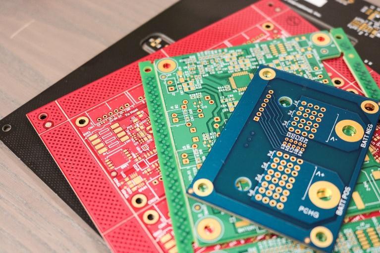
Fig 5: PCBS with colored solder masks
On the solder mask, the PCB presents a layer of inscriptions called silkscreen.
The silkscreen is a layer of ink trace that marks text and symbols on PCBs to identify the position of components (based on the reference designator) and to specify the orientation of components.
One word of caution: it is important to avoid overlaps of the silkscreen on the pads as observed in Fig 6 as they can create issues during soldering, with potential disastrous consequences in the long term.
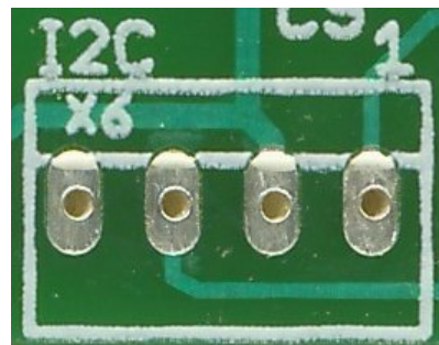
Fig 6: Silkscreen overlap
The most common finish for the solder pads in use today are: Hot Air Solder Level (HASL), Lead-Free HASL, Immersion Silver (Au), Immersion Tin (Sn), Electroless Nickel Immersion Gold (ENIG), and Electroless Nickel Electroless Palladium Immersion Gold (ENEPIG). These are listed from the least to the most expensive technology.
Simply put, better finishing gives a straighter surface for the pads that allows for a better soldering of components on the pads.
ENIG is a long-proven industry standard and is readily available from most PCB fabricators. ENIG deposits have tighter, more uniform grain and maintain high solderability, while also resisting corrosion.
The most common stackup in use today is a 4-layer stackup with ENIG finish and green solder mask, where the two middle layers are dedicated to “power” (VCC or multiple combination of VCC values) and “ground” (GND).
The remaining outer layers are used for connections between components.
Now that we have an overall view of the PCB technology, let’s go over the various steps involved in the PCB assembly process. At NeuronicWorks, we provide end-to-end PCB design and PCB assembly services.
Pre-PCB Assembly
PCB design
Electronics designers turn functional requirements into “schematic diagrams” – symbolic recipes showing which electronic components will be used and how they will be connected to make a functional circuit.
Schematics are abstracted to contain the conceptual information of a circuit. The schematic “recipe” is then turned into a “PCB layout” – a set of drawings showing the physical aspects of electronics components and their connections in a way that can be manufactured.
Layouts include 2-dimensional drawings of each copper layer, drill hole (vias) information, stackup information, quality standard requirements, and 3-dimensional models of the final circuit board.
Designers use Computer Aided Design (CAD) software to enforce design rules and perform automated inspections so that the end-result matches the specifications of the schematics and meets manufacturing requirements.
The CAD software is used to convert the design into files for the board fabrication house (Gerber files), and for the assembly house (pick-and-place files and/or assembly files).
After this, a verification process (design rule check) is conducted to determine any layout mistakes before they can affect board functionality or manufacturing capability.
The design goes through a DFM (Design for Manufacturing) and DFA (Design for Assembly) check for quality, accuracy, modularity, and consistency.
PCB manufacturing
Once design verification is completed, manufacturing files need to be prepared that will have information in the style and format universally accepted by a PCB manufacturer.
Manufacturing files include Gerber files in specific formats, a netlist, fabrication drawings, assembly drawings, NC drill file, blind/buried vias information, Bill of Materials, and PCB panel drawings.
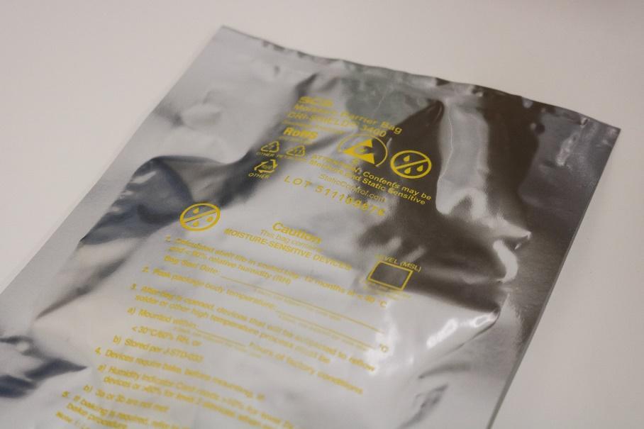
Fig 7: Moisture Barrier Bag (MBB)
Preparing PCBs and components
Once the PCBAs are manufactured and the components purchased, they need to be prepared for assembly purposes.
One of the preparation steps for reflow assembly is to assure that both the PCBAs and the components have a low level of humidity.
PCBs and moisture-sensitive components will have to be baked as a pre-treatment to dry them before assembling.
PCBA and components baking is a process performed in temperature-controlled ovens where the temperature and time of baking depends on the PCB and components thickness and exposure (standard J-STD-033).
Typical baking temperature ranges from 125 C to 150C and it can last for 24 hours. PCB Baking avoids issues like IC popping and PCB delamination that can occur if moisture is present on the board.
Moisture sensitive components must be vacuum sealed in a Moisture Barrier Bag (Fig 7) with desiccant (Fig 9) and a Humidity Indicator Card (Fig 10) and should be removed from the bag only prior to assembly.
Once removed, one has a window of 168 hrs to perform the reflow process (for MSL3 components). Beyond this point the components must be re-baked for assembly or storage purposes.
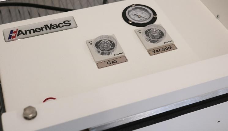
Fig 8: Vacuum machine for sealing
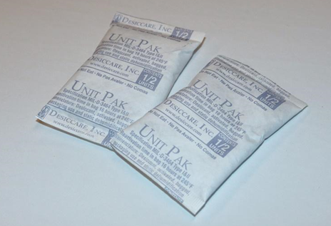
Fig 9: Desiccant
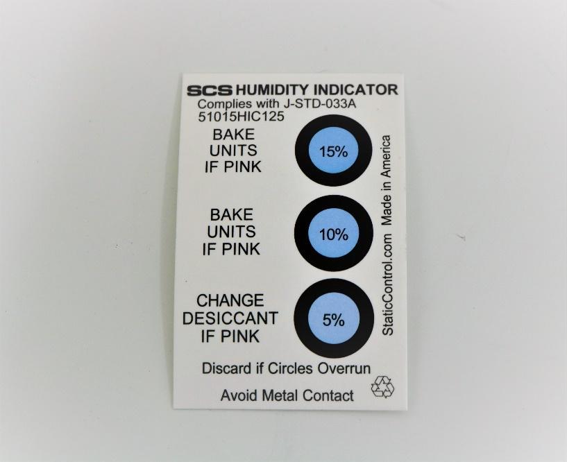
Fig 10: Humidity Indicator Card (HIC)
Preparing for PCB assembly
Before assembly, there are preparations that need to be completed to ensure a successful production run.
From the manufacturing files, the engineer must prepare work instructions, determine procedures, and create data logs.
Preparing for stencils is an important step in the case of screen printing. Stencils, as the term suggests, are thin sheets of material with apertures that correspond to component pads on a PCB.
Each PCB would require a unique stencil, and this method of solder paste application is especially useful in high volume production runs. I’ll discuss this more in the next section.
Next, the machine programs must be prepared per product. The programming is done based on mounting location information, length, width and thickness of PCBs, material information, among others.
One option is to do this preparation offline while the line is processing a previous run. The machine program is set up offline to quickly load for the next run without losing time.
In the case of special applications, prerequisites need to be determined and planned for in advance.
For example, in the case of Flex PCBs it is important to consider an SMT pallet that will help support and transport the flex PCBs through the SMT process.
PCB Assembly
Solder paste application
The fabricated board initially goes through solder paste application on the designated pads.
The solder paste is a combination of metal solder particles and flux that helps clean the soldering surface of impurities and oxidation. It also acts as an adhesive to bind the electronic component to the printed circuit board.
Solder paste application is done either by screen printing the paste through stencils or through the more advanced, non-contact method of jet printing. Once applied, the stencil must be cleaned and used for the next board.
For every new design, a new stencil would have to be built, which can be quite expensive especially in the case of low and medium production levels.
Jet printing, on the other hand, is a non-contact method that deposits an accurate amount of solder on each surface mount pad and allows for solder application of about 40,000 pads per hour, with a dispensing speed of more than one million dots per hour.
The technology builds up paste volume by applying single dots to achieve the right amount for each component.
Jet printing is better suited for special applications like pin in paste, paste in cavities, etc. where 3D features of a PCBA cannot be served by a 2D technology (stencil application).
Though jet printing has gained a lot of momentum because of the inherent benefits it offers, like quicker changeovers and no requirement of stencils, in the case of high-volume production, stencil-based screen printing is still the preferred method of solder paste application.
And in the case of designs with a mix of large and very small components, where it is a challenge to apply the right amount of solder in one setting, screen printing along with a combination of jet printing is an ideal solution.
After solder paste application, special considerations must be made for heavier components. Usually, the heavier components are left to be soldered in the second pass of the reflow process.
However, if they end up being on the bottom side of the board, going through the oven for the second time, they will have to be glued in place to avoid displacement due to gravity.
To accomplish, before component placement, drops of SMT adhesives are added (manually/automatically) corresponding to the position of the bigger components.
Solder paste inspection
After the paste application by either method, for high volume requirements, Solder Paste Inspection (SPI) is conducted to ensure the alignment, volume, and quality of solder paste deposit.
Improper solder paste printing can result in solder joint defects that lead to rejects. Excess paste can result in shorts and bridges, while insufficient paste will not create the required electrical connection.
Pick-and-place components
After solder paste application, the next step is to place the components on to the solder contacts.
For SMT technology, this process is handled by pick and place machines that offer high speed, high precision placement of a broad range of electronic components like capacitors, resistors, ICs and more.
Surface mount components are supplied to the machines in tape reels or trays that are loaded onto feeders mounted to the pick and place machines.
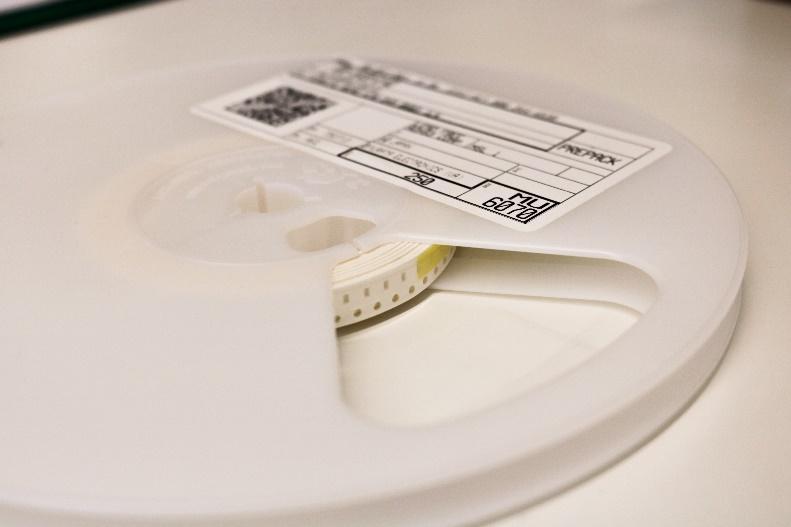
Fig 11: Components (resistors) in tape and reel packaging
Based on the PCB design files, the pick and place machine will pick each component (with pre-programmed X-Y coordinates and rotation) using a vacuum pipette, pneumatic suction cups or grippers from its tray or reel, and places it carefully on the exact solder paste applied position on the board.
Today, the fastest pick and placement machines offer placement speeds of up to 250,000 CPH (components per hour) for optimized combinations of a few PnP machines.
The component placement accuracy, completeness, orientation and polarity will be inspected during this stage.
Reflow soldering
Once the components are in place, they must be soldered to firmly attach to the contact pads. In this process, the PCBs are moved into a reflow oven where the solder paste melts and bonds the components and contacts under high heat, creating solder joints.
It has become common practice for miniaturized PCBAs to inert the atmosphere during the soldering process using nitrogen. A nitrogen-based reflow environment minimizes chances of oxidation on soldered surfaces.
Longer reflow ovens will have more temperature zones that will allow for a smoother temperature transition between zones recreating the recommended solder profile with better results.
A standard reflow oven has four temperature zones (see picture below):
- Preheating zone: The solder paste is activated at this temperature.
- Absorption/Thermal soak zone: The temperature of various components stabilizes at this temperature.
- Reflow zone: Temperature is at the highest at this zone and is when the solder pastes completely melt. The time in this zone should be less or it may cause damage to the PCB/components.
- Cooling zone: The temperature is cooled below the solidification point of the solder paste to solidify solder joints.
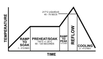
Fig 12: Temperature Zones in a reflow oven (Image source)
The temperature across these zones must always be controlled at an appropriate range to avoid damage to components and welding/soldering quality.
It is prudent to also mention that today, mostly all lead solders are being phased out due to its negative environmental and health effects and RoHS compliant lead-free solders are more commonly used.
This step completes the PCB Assembly process.
Post PCBA Quality Control
Manual inspection
Though not the most reliable method of inspection, we mention this here because the boards need to be manually inspected by the PCBA technicians at every step of the assembly process.
This is especially feasible for lower component density boards and can be challenging with advanced SMT boards.
Automated optical inspection
The AOI method uses multiple, high-resolution cameras installed at different angles to detect board defects and solder defects. AOI imaging technology has evolved from 2D (for simple inspection, measurements, or orientation detection) to 3D imaging that offers precise data.
This method of inspection detects board defects such as wrong/missing parts, incorrect orientation and polarity, and tilted (known in industry as tombstone) or flipped components.
It also detects solder defects such as no/insufficient solder, excess solder, or solder bridge.
Despite the popularity of 3D imaging, AOI systems are more efficient when they employ both 2D and 3D inspection technologies.
X-ray inspection
X-Ray inspection is generally used to test the quality and accuracy of PCB soldering for complex high-density chips, in cases where optical inspection cannot be applied.
When applied, the X-ray can determine how precise the solders are and can detect defects hidden beneath IC packages.
Defects detected include excess solder (shots, bridges), open solder joints, lifted pins and misaligned joints, etc.
It is the preferred detection method for high density components like BGA, as this technology allows you to see “inside” the PCB assembly.
Testing
After PCB Assembly, the final PCB should be tested by a QC engineer to identify any issues or flaws.
There are mainly two types of testing, flying probe testing and Test-jigs. Flying probe is the preferred testing method for low volume, critical application PCBAs (military, transportation, aerospace).
This test involves the use of several electric probes, automatically brought in contact with the board, that are applied to the board. Some provide external stimuli and some read the response of the board.
It is a very engineering intensive process to plan the test, program the machines, and perform the test. The flying probe machines are generally very expensive and are usually preferred to test PCBAs aimed for critical applications.
For mass production, test jigs are a better choice. They are specialized or customized testing platforms for unique PCBAs. Using static probes, electrical signals and power is applied to the PCB and outputs are checked and measured.
This test will ensure the PCB meets the electrical requirements specified in the design. The test can take from a few seconds to a few minutes.
In addition to testing, the final firmware for production can also be loaded on the board at this stage.
Preparation
After testing, the boards are cleaned using the ultrasonic cleaning method which aims to wash off any flux, resin or solder residue, dust or dirt that could have accumulated during the assembly process.
Post cleaning, the board is ready for conformal coating where a thin layer of protective coating material is applied on the board to prevent moisture contamination, erosion, oxidization, etc.
It protects the PCBs from mechanical vibration, thermal shocks, and other adverse environmental condition effects.
Finally, the PCBAs are now ready to be packaged and shipped. PCBAs are usually packaged in antistatic bags.
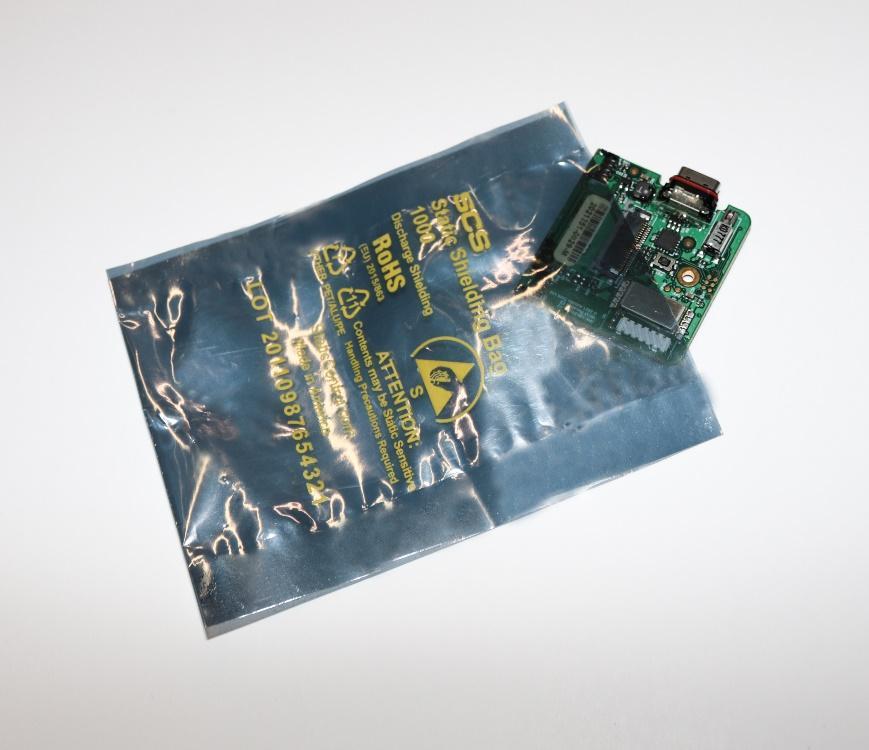
Fig 13: PCB to be packed in antistatic bags
Design for Assembly
It wouldn’t be wise to end this blog without mentioning the Design for Assembly principle.
With NeuronicWorks being vertically integrated as both a design and manufacturing house, the Design for Excellence (DfX) principles are ingrained in our design culture here.
We know how important it is to design with the vision of manufacturing, assembly, cost, reliability, testability, serviceability, supply chain, regulatory compliance, innovation, recyclability, etc.
In the case of PCBAs, if the initial PCBA design focuses exclusively on the board without factoring in the application, use-case or system environment, then that PCBA fails to design for assembly.
In isolation, the PCBA design may be perfect, but there are other issues to consider – are components available for production orders, what is the size and quantity of components being used, are they ideal for production in large quantities?
The primary objective of Design for Assembly (DFA) is to eliminate complexity and reduce uncertainty while boosting efficiency.
With this principle in mind, designers are encouraged to think of the big picture and to think of design implications at every stage.
The PCBA design decisions made by a designer will not just have an impact on PCBA assembly, but also have a direct impact on the form, quality, and reliability of a completed product.
