
Introduction to Transistors
The circuits I’ll cover in this article are more complex than previously discussed. You will learn about the functionality and applications of bipolar-junction transistors (BJT) and field-effect transistors (FET).

In my previous article Introduction to Basic Electronics Circuits you were introduced to the simplest, most basic types of electronic circuits. This is a great place to begin the journey of learning electronics, but ultimately any real-world circuit will be more complex than those discussed in that first article.
In that article I focused on what are called passive circuits. Passive components include resistors, capacitors, inductors, transformers, etc. An active circuit on the other hand uses more complex components like transistors. An electronic component is considered active if it allows the device to control the current in other parts of the circuit.
The circuits I’ll cover in this article will be more complex, but they are still all relatively simple circuits. I don’t want to overwhelm you and it’s critical to start simple and slowly work up to more advanced circuits.
There are two broad classifications of transistors that we’ll be analyzing: bipolar-junction transistors (BJT) and field-effect transistors (FET). Transistors can either be operated as digital switches, or used in analog applications such as amplifiers and power regulators.For this introductory article I won’t get into the low-level physics of these transistors which will likely only cause confusion, and instead the focus will be on their functionality and applications.
Bipolar Junction Transistors (BJT)
Let’s first look at bipolar junction transistors which are so named because they are made of two diode junctions. A bipolar transistor comes in two flavors: NPN and PNP. The N and the P refer to whether the area of semiconductor silicon is doped negatively or positively.
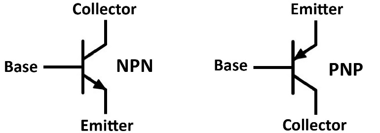
Figure 1 – Bipolar Junction Transistors (BJT) (n-type = NPN, and p-type = PNP)
A bipolar transistor consists of three pins: collector, base, and emitter. For an NPN bipolar transistor the current will flow from the collector to the emitter. For a PNP transistor the current will flow from the emitter to the collector.
For an NPN transistor to be turned on the base voltage must be greater than the emitter voltage. The opposite is true for a PNP transistor where the base voltage must be less than the emitter voltage.
In most circuits the emitter of an NPN will be tied to ground (or tied to a resistor that connects to ground), and the emitter of a PNP will be tied to the positive supply (once again possibly through a resistor).
A bipolar transistor has three regions of operation:
Active region:
When operating in the active region the transistor acts as an amplifier. The voltage between the base and emitter pins (commonly called Vbe) controls the amount of current that flows between the collector and the emitter.
This is an exponential relationship so the smallest change in Vbe can have a huge impact on the collector current. Since this base-emitter junction is really just a diode the voltage (Vbe) will always be close to 0.7V. This relationship is governed by the following equation:
IC = IS * exp (Vbe/VT)
Where IC = collector current, IS = reverse saturation current (a known constant on the order of 10−15 to 10−12 amperes), and VT is called the thermal voltage which is proportional to temperature (approximately 26mV at room temperature).
A bipolar transistor operating in the active region also provides current amplification. The current flowing through the base pin will be gained up by a transistor parameter known as β (beta) or sometimes hFE. This gained up current will then flow between the collector and the emitter. The equation for this is:
IC = β * IB
Where IC =collector current, β is the current gain specification for the transistor, and IB = the base current.
Finally, the emitter current for a BJT is equal to the sum of the base and collector currents:
IE = IC + IB
Saturation and Cut-off:
In the saturation region a bipolar transistor is fully on and acts as a closed switch between the collector and emitter pins. Whereas, when in the cut-off region the transistor is fully off and acts as an open switch.
However, for digital switching applications I prefer to use field-effect transistors instead of bipolar junction transistors.
Field Effect Transistors (FET)
The other broad classification of transistors are called field effect transistors. Just as with a BJT, a FET has three pins that provide similar purposes. The control pin is called the gate (instead of base). The current in a FET flows between the drain (similar to the collector on a BJT) and the source (same as BJT emitter).
One of the most significant functional differences between BJTs and FETs is that the control pin (gate) is electrically isolated by an insulating oxide layer. No current flows into the gate as it does with the base of a bipolar transistor. A FET is purely a voltage-controlled device.
As with bipolar transistors, FETs come in two flavors: n-type and p-type. There are various types of FETs available, but the most common type are called MOSFETs. The MOS stands for Metal-Oxide Semiconductor and it simply refers to the insulating material that forms the isolated gate.
An n-type FET is commonly called an NFET, or an NMOS for n-type MOSFETs. A p-type FET is called a PFET, or a PMOS for p-type MOSFETs.
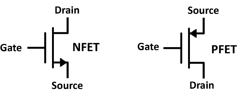
Figure 2 – Field-Effect Transistors (FET) (n-type = NFET, and p-type = PFET)
Field-effect transistors have three regions of operation:
Cut-off region:
An important parameter of a FET is what is known as the threshold voltage (Vt). This is the minimum voltage between the gate and source pins (called VGS) at which the device begins to turn on. If VGS is less than Vt then no current will flow between the drain and source. This region is known as cut-off or subthreshold mode:
If VGS < Vt then Id=0 (cut-off region)
In the cut-off region a FET acts like an open switch.
Once VGS becomes larger than the threshold voltage (Vt) then the FET will enter either the linear region or the active region depending on the voltage between the drain and source pins.
Linear region (also called Ohmic mode or triode mode):
When VGS is greater than the threshold voltage, yet the voltage across the drain-source pins is less than the difference between VGS and Vt, then the FET is operating in the linear region.
If VGS > Vt and VDS < VGS – Vt = Linear region
When in the linear region a FET acts as a voltage-controlled resistor. In this region, if the gate voltage is large enough then the FET will act like a closed switch (i.e. low resistance resistor).
Active region
When VGS is greater than Vt, and the drain-source voltage (VDS) is greater than the difference between VGS and Vt, then the FET is in the active region.
If VGS > Vt and VDS > VGS – Vt = Active region
When in the active region the FET can perform functions such as voltage amplification.
A bipolar transistor is known as an exponential device because of the exponential relationship between the output current and the control voltage (Equation 1) when operating in the active region.
On the other hand, a FET is a square-law device meaning the output current is proportional to the square of the control voltage (VGS) when operating in the active region. The equation for a FET is as follows:
ID = k’ * (VGS – Vt)2
where ID = drain current, and k’ is a constant associated with the particular FET.
This has only been a very basic introduction to some of the fundamental concepts associated with transistors. Depending on how deep you want to go there is much more to learn. In fact, many books have been written that cover transistor physics and/or transistor circuit design.
Now that you have a basic understanding of bipolar and field-effect transistors let’s put them to some use by connecting them up to form an electronic circuit.
Transistor switches
A simple and common use for a transistor is to turn on and off an LED indicator. The circuit below shows how a bipolar NPN transistor and an NFET transistor can be used for this purpose. The square wave signal shown below may be an I/O pin coming from a microcontroller.
Many microcontrollers can source/sink a few milliamps of current so in some cases you could simply wire the LED directly to the I/O pin without the need for a transistor. But in cases where you need an LED current higher than your microcontroller can support then you would use a transistor switch.
![]()
Figure 3 – Transistor LED driver switches
When the square-wave signal (control voltage) is high then Q1 (bipolar NPN) and Q2 (NFET) are both fully turned on and appear as a closed switch. This allows current to flow through each LED. The resistors in series with the LEDs are used to set the current level that flows when the transistors are closed.
Note the resistor (R4) in the base of the NPN transistor. A base resistor like this is required on a bipolar transistor so as to limit current and prevent damage. Remember, the base-emitter junction on a bipolar transistor is just a diode.
As you likely already know a diode requires a current limiting resistor, and this is true with bipolar transistors as well. The voltage across the base-emitter junction is very close to 0.7V, so if you were to try to put 5V across this junction (without the base resistor) then it would cause serious damage.
Transistor inverters
An inverter is one of the simplest circuits that you can design. An inverter takes a 0 and turns it into a 1, or vice-versa. We’re going to look at using only FETs to build an inverter.
The circuit shown in Figure 4 is just two inverters. The first inverter is formed from Q1 and R1, and the second inverter uses Q2 and Q3. Q1 and Q3 are NFETs, whereas Q2 is a PFET.
If the gate of an NFET is high (compared to its source pin) then the transistor is fully on and looks like a closed switch. When the gate is low then the FET is full off and looks like an open switch.
A PFET is just the opposite. If the gate is low, then a PFET is turned on. If it’s high, then it’s turned off. For a PFET the source will likely be tied to the positive supply.
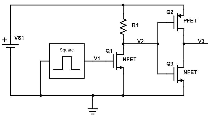
Figure 4 – FET digital inverters
When V1 is zero, Q1 is turned off and looks like an open circuit; that means the voltage at node V2 gets pulled up to the supply voltage at the top through resistor R1 because now Q1 is off. If V1 is high, now Q1 is turned fully on which pulls V2 to ground.
So if V1 is zero, V2 is one. If V1 is one, then V2 is zero. That’s an inverter.
A better way to make an inverter though is by replacing the top resistor (R1) with a PFET. The problem with using a resistor for the pull-up function is that the pull-up current will be quite small. A small pull-up current means the output of the inverter will be slow to change from a zero to a one.
The response of this first inverter will be asymmetrical. It will pull node V2 down really quickly through Q1, but it will be much slower to pull V2 high. This problem is eliminated by using a PFET instead of a resistor for this pull-up function.
For the NFET/PFET inverter (Q2 and Q3), when it’s input voltage (V2) is low, the NFET is turned fully off and the PFET is turned fully on. So the output voltage (V3) will be high.
On the other hand, if V2 is high, now the PFET is turned off and NFET is turned on, so V3 is pulled low. You put a one in, you get a zero out. You put a zero in, you get a one out. It does the same function as Q1 and R1, but with symmetrical rise and fall times on the output.
Bipolar transistor circuit
Finally, we’re going to look at a circuit with a bipolar transistor, or specifically an NPN.
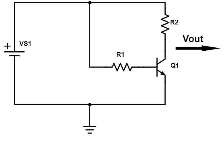
Figure 5 – Simple NPN circuit
As previously discussed in Equation 2, Beta is the current gain for a bipolar transistor. For example, if Beta is 100 and the base current is 1uA, that means the collector current will be 100uA, and the emitter current will be 101uA.
For the circuit shown in Figure 5, the current flowing through R1 into the base gets gained up by the Beta, and then that flows through R2.
If you wanted to calculate the output voltage of this circuit, the first step is to calculate the base current. To do this you need to find the voltage drop across R1, and then use Ohm’s Law to calculate the current. The left side of R1 ties to the supply voltage, and the right side goes to the base of the NPN.
Remember, the base-emitter junction of a bipolar transistor is just a diode junction with a voltage of approximately 0.7V. So to calculate the base current you would use the following equation:
IB = (VS1 – 0.7V) / R1
To calculate the collector current you simply multiple the base current by the transistor’s Beta as previously shown in Equation 2.
The current flowing through resistor R2 is equal to the transistor collector current. To calculate the output voltage of this circuit you now need to calculate the voltage drop across R2 and simply subtract that from the positive supply voltage:
Vout = VS1 – (IC * R2)
This is a really simple circuit that doesn’t have much real-world use but it introduces you to some of the fundamentals of bipolar transistors.
Conclusion
This article has introduced you to the very basic concepts of active transistor circuits. The types of circuits that can be built using transistors are really quite breathtaking. Transistors are at the heart of every electronic device.
That being said, since the invention of the Integrated Circuit (IC) the need to design complex, discrete transistor circuits has been reduced mostly to engineers designing IC microchips.
However, there is still a need for a basic understanding of transistors, and many designs will use a few discrete transistors. But most designs now tend to use integrated circuits instead of discrete transistor circuits for any complex functions.
Unless you plan to become an IC designer you will likely only need an introductory understanding of transistor circuits.
If you enjoyed this article please share it or if you have any questions just leave a comment below and I will answer your questions.

Hi John,
The figure you made for the transistors and FET’s has an error on it. The labels between the “N-FET” and “P-FET” should be swapped. A P-FET’s “arrow” points outwards, not inwards.
Thanks for the comment Tobias. Actually the symbols I have are correct. The arrow that you maybe have seen elsewhere for an NMOS with an arrow pointing inwards is for the body connection, not the source. If you use the 3 terminal symbol without the body connection then the arrow is on the source and points outward for an NMOS, and inward for a PMOS. Hope this clarifies it better for you.
Thanks John. Very clear and concise presentation of a confusion subject to some , including me.
Thanks Todd!
Muy buen articulo. Ojala y tenga un escrito del transistor IGBT.
Gracias!
Best electronics and design website I have found. Before I found this website I was struggling to find any information. But know I can get everything in one place. I learned a lot about you article about molds and their design. I am an Electronics freelance designer.
Thank you Kelvin! I’m very happy to hear that my site has proven helpful to you.
Yes, that makes it all quite clear, each part separately is an inverter. Thanks as always!
Hi John,
Your articles and advice are always so valuable, thanks for the effort. This one has helped to fill in my scant knowledge of transistors, especially the difference between BJT’s and FET’s. I always wondered what made them different, now I know!
I understand the first inverting function in Fig.4, but it seems like the secondary array of one PFET and one NFET would invert the signal again, at least as you have it drawn. It seems like trading their positions would carry the signal thru without inverting again, but have the faster pull-up response you mention is their purpose. Have I got this wrong? Please enlighten me if I do.
Cheers,
Chris Corkins
Thank you Chris for the great feedback!
As for the inverters I meant for each to be considered separately. You are correct two inverters just cancel out. I should have probably drawn them as two unconnected inverters. Does that clear up your confusion?
Pretty good balance of information without overwhelming. Just wanted to note there are a few typos just above figure 2. (Mind your P’s and Q’s … errrr N’s!)
Nice job.
Thank you Alan! I just fixed those typos. Thanks again.