
5 Steps of Product Development for a New Electronic Hardware Product
The product development process for a new electronic product (or any physical product) is by no means simple. Since it can be pretty overwhelming, I’ve broken product development down into five manageable steps.

The steps summarized below will get you to the point of having a fully functional prototype. However, after the prototype is completed, there are still many other steps to getting a product to the point of being ready to manufacture and bring to the market.
The purpose of this article is to focus on the five core steps required to develop the prototype for a new electronic product.
Step #1 – Design the Circuit Schematic
The end goal of the electronics design is the creation of a Printed Circuit Board (PCB). The first step of making a new PCB is the creation of the schematic circuit design. A schematic is similar to a blueprint for a house.
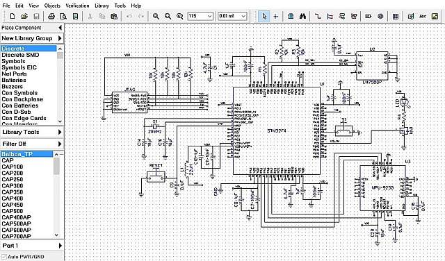
A schematic circuit diagram is the first part of designing a new electronic circuit board.
Designing the schematic circuit first includes early research to select the best topology and most affordable components.
It may also include running simulations and/or breadboarding (used only rarely in modern electronics).
Step #2 – Design the Printed Circuit Board (PCB)
Using the same software package as in step #1, the designer now creates the PCB layout.
A portion may be automatically routed but most boards require manual routing for optimum performance. The PCB layout is extremely sensitive for power and RF circuits (Bluetooth, WiFi, GPS, etc) and mistakes on the PCB in these areas are common.
After the schematic diagram is done it’s now time to create the PCB layout.
When the PCB layout is complete the design software will tell the designer if the PCB matches the schematic. It will also check wire widths, trace spacings, etc. to ensure the layout meets all of the rules for the particular PCB fabrication process being used.
Before beginning the PCB layout it will be necessary to obtain all of the specification from your PCB manufacturer for their process. Each PCB manufacturer has different specifications for their process.
Once the PCB design is completed it’s time to send the data off to a PCB shop for prototyping. You can expect the boards to arrive in about 1-2 weeks (without paying extra for rush service).
To learn more about PCB design be sure to watch this free tutorial and check out this in-depth paid course which teaches you every step of PCB design.
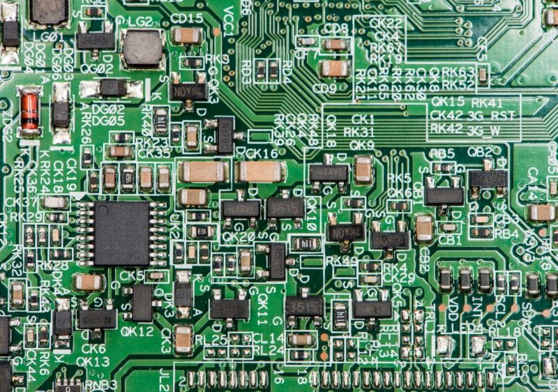
Step #3 – Evaluate and Debug the Prototype
Once the first prototype comes back it will now need to be evaluated and if any problems are found, those will need to be debugged.
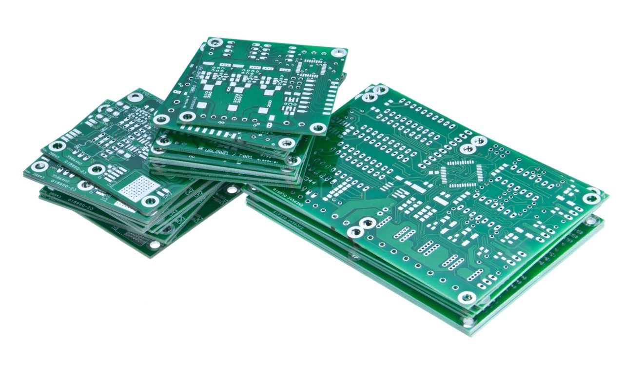
Examples of blank (before components are soldered on) Printed Circuit Boards (PCBs).
Hopefully there are no problems, but that’s extremely rare, and there are almost always at least a couple of issues.
Debugging a new circuit is a difficult step to forecast, because until you know what the problem is, you can’t estimate how long it will take to fix it.
Step #4 – Program the Microcontroller
Almost all electronics products today have some kind of microcontroller that acts as the brains for the product.
These are almost always programmed in a computer language called “C”. If the program needs to be super efficient or fast then parts of it may be done in assembly language.
Sometimes the programming will be done by the same person that designed the circuit, but many times a software specialist is brought in to do the programming.
Step #5 – Design the Enclosure
This is almost always handled by a different engineer than who did steps 1 thru 4.
In the beginning all you really need is a 3D modeling expert, especially if you have a good vision of what your product should look like.
Eventually you may want to hire an industrial design engineer to really make it look good. For example, industrial designers are the engineers responsible for making Apple’s products look so cool.
Either way make sure whoever does the 3D model design has experience with injection molding technology. 3D printing is used for low-volume prototyping, but injection molding is used for high-volume manufacturing. It’s a common mistake for 3D designers to create a model that can be 3D printed but not injection molded.

thank you for share the informative blog article.
Thank you for the comment Gwen, I hope you found it helpful!
Fabulous post, you have denoted out some fantastic points, I likewise think this s a very wonderful website. I will visit again for more quality content and also, recommend this site to all. Thanks.
thanks for sharing this article with us, your article is very helpful for me being a student
Thank you for sharing these steps.
Thanks for providing us this valuable information these types of information is very helpful for me
another question would be , How to certify the product in order to sell it ???
Hi Albert,
For certifications please see this article.
As a student I can do all of the circuit analysis and math to find gain or frequency cutoff of a given circuit, but this taught me some of the thought process behind the choices made. Thanks.
Thanks for providing us this valuable information these types of information is very helpful for me and this step by step information help me for understand easily and fully. Keep share thesee information with us.
Product style and development have come back to a protracted method from ancient development.
Earlier, development concerned a semi-conductor company building a reference style around a brought-out silicon/processor and promoting it within the targeted market section.
I’m creating a device that can show a real time camera view and be connected to a phone via App programming what kind of components help you efficiently connect? I have no idea where to start but this information has been solid. Thank you! I’m about to start learning Electrical Engineering wish me luck!
Product style and development have come back to a protracted method from ancient development.
Earlier, development concerned a semi-conductor company building a reference style around a brought-out silicon/processor and promoting it within the targeted market section.
vapedubai.org
Thanks for providing us this valuable information these types of information is very helpful for me and this step by step information help me for understand easily and fully. Keep share thesee information with us.
Thank you Ishan for the feedback.
Best wishes!
Hi.
I am here to design a product which is based on electronics. How I have to proceed for that to get the end product.
I like how you mentioned that a schematic is similar to a blueprint for a house. I’m sure having an accurate and detailed drawing is critical in creating anything like a circuit board, equipment, or other shop items. It’s amazing at what can be created from just a drawing or schematic.
Hi,
I am trying to do a school project where I have to design something to be used in sport. I have the idea but need to show costs for the project. Can you give me a ball park figure to use in my assignment for a simple PCB with a small hand held casing ?
Thanks
Simon
Hi Simon,
Thanks for the question. See these two articles for more details. Note that there is no standard answer and every product is different.
https://predictabledesigns.com/how-much-will-a-prototype-cost/
https://predictabledesigns.com/the-cost-to-develop-scale-and-manufacture-a-new-electronic-hardware-product/
Best wishes,
John
I’m really surprised that the design doesn’t start with the mechanical layout-with the positioning of the mounting hole locations and interface components.
Aside of prototypes, I’ve seen very few electronics components that were self-contained packages.
I find that I have followed this process several times in the past only to have to completely redesign the PCB to fit into to case that is required for ergonomics and functionality.
Now, I take the approach of designing a basic case first, and the PCB is usually the more flexible of the facets in the product. Once I know what shape and size the PCB needs to be, then I can work on the detailed layout.
For many products the PCB is quite a bit smaller than the case, resulting in little interaction between the mechanical design and the PCB layout, but for others they are coupled, so the shape and layout may be affected.
Thanks for the comment Keith. It’s important that you have a rough idea on the size of your product and you don’t want the PCB layout designed with no limits at all on size or shape. Some product inventors know exactly the size they want, and in those cases I work backwards from their case size. Some projects don’t have the size specified so clearly and the PCB size is a bit more flexible. Finally, some projects want a size that is too small for the electronics, so the size usually has to be increased to accommodate the required size PCB. If small size is super critical then advanced PCB production techniques like blind vias and high layer counts can be used.