
21 Design Mistakes to Avoid on Your PCB for Mass Manufacturability
Learn how Design-for-Manufacturability (DFM) and Design-for-Assembly (DFA) help prevent possible design mistakes before moving to production, making your development process more cost-effective and efficient.
In manufacturing, nothing is worse than discovering a design flaw during the manufacturing or assembly stage.
Refurbishing the board at this stage will increase the cost and put the board production on hold, and delay getting your product to market.
Hence, it is necessary to ensure that your design has minimum errors before moving to the manufacturing process.
The best way to do this is to apply Design-for-Manufacturability (DFM) and Design-for-Assembly (DFA) rules when designing your circuit board layout.
Now, let’s take a look at three of the most important things for building a PCB that can be efficiently manufactured without defects.
PCB Design-for-Manufacturability
Design for Manufacturability (DFM) is a set of guidelines to identify the possible errors in a circuit board.
Rectifying these problems during the design stage can make the board production more efficient and avoids any delays in the production process.
Usually, every manufacturer has a unique DFM checklist that they follow.
NOTE: In this article the manufacturability in DFM is referring only to the production of the bare circuit board. But, DFM can also refer to the enclosure, and the finished product.
Below are some of the most common PCB DFM design mistakes that you need to watch out for:
Incomplete and invalid design files
Whether it’s Gerber or ODB++, the input files carry vital information like layer images, board outlines, IPC netlists, master drawings, and layer order.
Any confusion in specifications can create a problem in later stages. Therefore, cross-check all the mandatory files before submitting them for production.
Inappropriate substrate material
Some circuits require special materials depending on their functionality. For example, a typical substrate will not work well with high-frequency signals.
Discuss the material requirements with your manufacturer and choose a suitable PCB substrate material in the initial stage.
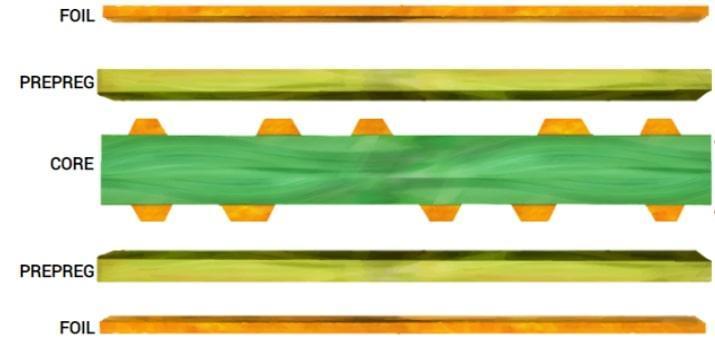
Materials for PCB fabrication
Improper trace widths
Copper traces connect all the components in your circuit. Any defects in traces can cause shorts, signal distortion, and heat dissipation.
The current carrying capacity of a conductor (trace) increases with its width.
If a higher current flows through the line, the heat dissipated will be more which can cause the board to overheat.
Therefore, optimize the conductor width according to your circuit requirement, and be sure to keep the trace width on the outer layers more than 4 mils.
You can optimize the trace width, current capacity, and temperature rise using online tools.
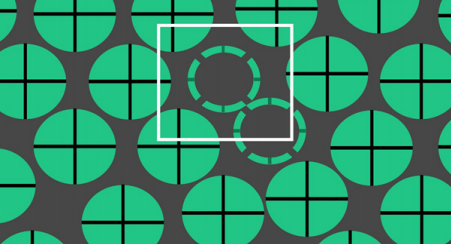
Improper trace spacing
Also be sure to not compromise the conductor spacing in an effort to make the circuit layout more compact.
Smaller gaps between the traces can result in flashovers and crosstalk between them.
You should follow the standard guidelines and provide sufficient clearance between conductors.
Like trace width, you can compute the optimal spacing between the conductor using conductor spacing and voltage calculator.
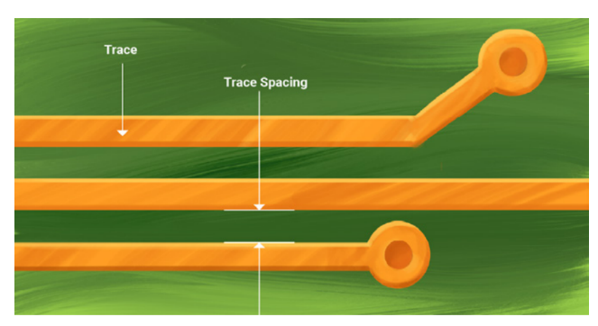
Copper trace spacing illustration
Acid traps
During trace routing, if any line forms an acute angle (below 90°), it creates an acid trap.
The residual acid can get trapped in the bent region during the etching process, and this can cause an over-etch of the trace.
Avoid acid traps by preventing acute-angled bends while routing as shown in the below image.
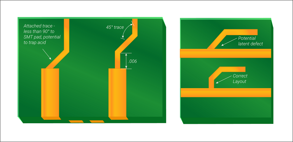
Acid trap formation
Inadequate trace-to-edge spacing
You should maintain an optimum spacing between the edge and the trace in the circuit layout. If you reduce the space for any reason, the outer copper conductor can get partially shaved or cut during the depenalization process.
Insufficient spacing between copper and board edges can lead to exposed copper and burrs along the edges.
Drilling process errors
In printed circuit boards, the manufacturer drills holes for various purposes like vias, alignment, component placement, etc.
Drilling is an irreversible process, and any undesired drill can ruin your design.
Other things to consider are size, spacing, aspect ratio, number of holes on board, and type of machine (laser/ mechanical).
Common errors which affect drilling are insufficient annular ring and drill to copper distance. Contact your manufacturer and learn about their drilling technology and specifications.
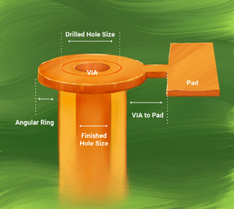
Specifications for drilling vias
Faults in annular rings
An annular ring connects a via to a trace. If the diameter of the annular ring is insufficient, it will disconnect the signal flow between the conductor and the via.
The finished drill hole may have a tolerance of ±2 mils, so an annular ring can show a breakout when it is less than 2 mils. This can cause an open circuit.
Apart from this, an insufficient annular ring of a component hole can lead to poor solder joints post assembly.
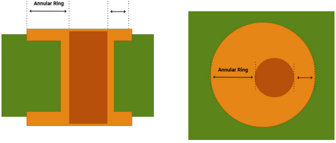
Annular ring placement
Solder mask errors
A solder mask on a PCB protects the surface from contamination and insulates the connections.
The manufacturer unmasks the areas where the components are placed (footprint and pads) for the soldering process.
If there is no proper clearance between the via mask opening and the adjacent component opening, it can create a solder bridge during assembly. This results in poor and inefficient solder joints.
Therefore, it is essential to maintain the required solder mask dam between the via opening and adjacent component opening.

CAM snapshot of a solder bridge
On the other hand, an inadequate solder mask can lead to the formation of a solder opening, and the exposed copper will be susceptible to corrosion.
Copper and solder mask slivers
Copper slivers are loosely bonded, thin, residual copper segments formed during the printing stage.
During pattern plating, these loosely connected slivers will lift off and fall into the plating bath.
These photoresist slivers can co-deposit anywhere on the board, leading to shorts.
Along with this, the areas where the photoresist gets removed will result in unwanted coppers on the board, which may affect the board’s functionality.
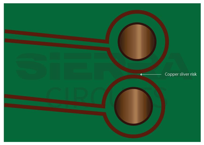
Copper sliver risk
Solder mask slivers are formed during imaging of the solder mask layer where the dams are maintained to avoid solder bridging.
When the dams are less than 4 mils, there is a chance that these loosely bonded dams become a sliver and wash away during the development stage.
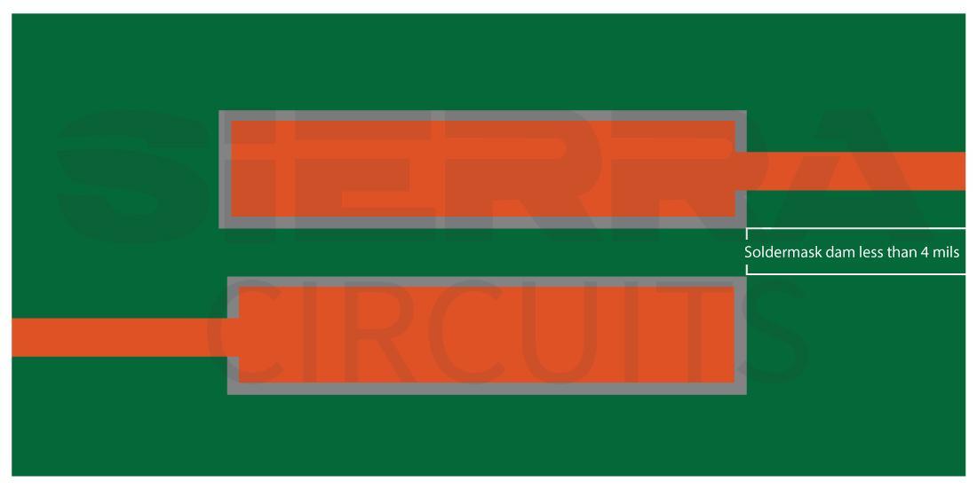
Solder mask sliver risk
Starved thermals
The soldering process generates excessive heat that can damage the board. To avoid this, you must provide sufficient thermal relief padding.
Thermal padding consists of small copper spokes called ‘thermals’ to aid heat conductivity.
If these thermals get disconnected from the pad or plane, they are called starved thermals.
These starved thermals can cause poor heat conductivity and overheat the board.
Disconnected thermals
Silk screen printing errors
Silkscreen is printed at the later stage of the manufacturing process. While printing, if the silkscreen overlaps on the pad, PCB surface, holes, etc., it can create problems in the assembly process.
For example, if the silkscreen is printed over the pad, it can melt into the solder joint and create a discontinuity.
PCB Design-for-Assembly
The Design for Assembly (DFA) process reduces the gap between the designer’s vision and the reality of the production process.
Here, you will check for component availability and placement. You also analyze the feasibility of production and other aspects crucial for an efficient assembly.
Understanding DFA, can help you simplify the PCB layout to reduce the project’s overall cost and lower the chances of design failure.
NOTE: In this article the assembly in DFA is referring to the process of soldering all of the components onto the PCB. But, DFA can also refer to the final assembly of the finished product.
Below are some of the most common DFA mistakes made on PCB designs:
Data inefficiency
Similar to DFM, you should verify all the essential data sheets before your design moves to the assembly process.
Verify the crucial parameters like package dimension, XY data, DNI specification, SI data, part number, etc.
By doing this, you can avoid future corrections and confirmations.
Choosing the wrong components
The selection of parts significantly impacts the assembly process.
For example, through-hole elements require a complex fabrication process when compared to surface mount technology (SMT).
Hence, it is best to use them only when needed.
Always pick standard over custom components, as standard elements are readily available with multiple vendors.
Since you can only procure customized parts from a selected vendor, they usually aren’t feasible for high-volume production and will also increase the cost.
Different types of components are available
Component availability
You should always confirm the availability of the parts before you build your bill of material (BOM).
If there is a supply shortage, you should be ready with an alternate component from a different vendor.
The BOM Checker can help you to get a cost estimation.
Incorrect footprint
The BOM specifies all of the components needed for assembling a circuit board.
If the size of the component specified in the BOM mismatches with the CAD footprint data, it will be challenging to complete the circuit. This will cause significant difficulties on automated assembly lines.
Rectification from this situation will be time-consuming and also increases the cost. Therefore, double-check the component size at the design stage.
Insufficient component spacing
During component placement, inadequate spacing can cause an overlap of parts, create solder bridges, etc. Providing an adequate gap between parts also facilitates manual soldering and rework.
Give special attention to the spacing of sensitive components like QFP/QFN, POP, or BGA.
Sometimes elements are closely placed to achieve a lower form factor. It is best to follow the spacing guidelines to ensure zero error in part spacing.
The below image shows the preferred component layout on a PCB.
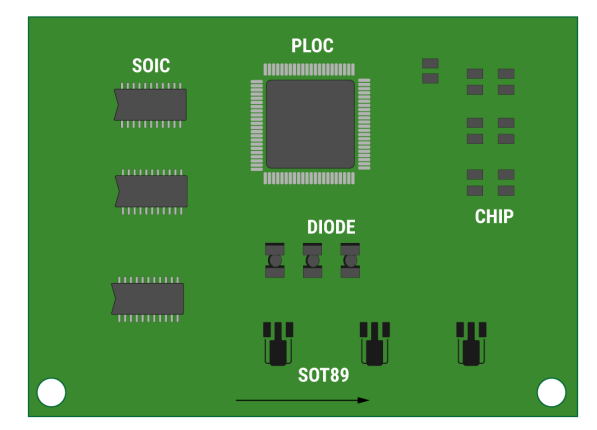
Standard component placement
Inadequate component to edge spacing
After completing the assembly process, the panels go through the depanelization process.
In this process, the parts at the ends of the board will have to handle high stress that might damage them. Hence, provide sufficient spacing between the component and the edge.
Additionally, the spacing options differ with the different assembly processes.
In manual assembly, you can place the units much nearer to the edge when compared to automated assembly.
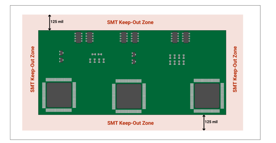
Standard component to edge spacing
Incorrect pad sizes and spacings
Choosing a smaller pad size can create poor solder joints in SMT components, and it can even break when applied to a through-hole part.
Making the pad size as large as possible may not be the solution. A larger width pad will take up more space and can make SMT components move from their position while soldering.
Similar to pad size, the pad spacing cannot be too close or far as they pose a problem while placing the components.
Silkscreen errors
The silkscreen layer contains lots of vital pieces of information. Some examples are component orientation marks, Pin 1 marks, polarity marks, cathode marks, etc.
If these details are missing or unclear, then assembly houses will waste time trying to confirm the correct data.
In the worst case, if the silkscreen has misprinted data like polarization and the assembler installs components accordingly, then the board might malfunction.
That’s why you need to ensure the silkscreen’s readability is good before the assembly begins.
PCB silkscreen printing specifications
High temperature errors
Fabricators need to take proper care during the soldering process since it can generate excessive heat that can damage the board.
Controlling the heat produced in this process is essential. Provide sufficient thermal padding for efficient heat dissipation.
DFM and DFA guidelines help you predict the design problems that can be easily fixed before the manufacturing process.
Even though they are not entirely foolproof, they will minimize the repercussions of design faults.
Never skip the design for manufacturing and the design for assembly steps if you want to improve your chances of building a quality PCB.
DFM check tools are available online to help you comprehensively analyze the board layouts.
Following these guidelines will help to ensure that you have a manufacturable PCB design, ultimately allowing you to get your product to market faster and cheaper.
This article was written by the team at Sierra Circuits.

Thank you for the detailed article, a lot of real world experience is needed to design and manufacture high quality PCBs that work reliably over time.
Thank you Max for the comment. And yes, you are correct:)