
How to Select the Best PCB Design Software for Your Project
This article will review various PCB design tools and help you select which one is best for you and your specific project.

This article is a guest post by Ryan Nelson who is an electronics design engineer. Be sure to checkout his YouTube channel EE for Everyone which has some fantastic tutorials on electronics design.
You’ve decided to design an electronic product, and now it’s time to design your circuit board! It’s easy to be overwhelmed by the number of software options when it comes to designing a schematic or circuit board.
This article will help you to understand what features you can expect from an Electronic Design Automation (EDA) tool. It will also help you to decide which software is best for you, discussing common features shared by many tools as well as differentiating features of specific tools.
What Is an EDA Tool?
Electronic Design Automation (EDA) tools are the latest version of a 20th century innovation. The first circuits were created before the Printed Circuit Board (PCB) was invented, and schematics were drawn by hand.
Through a combination of drafting tools, stencils, and careful manual process – a circuit diagram was drawn.
Over time, especially after the PCB was invented, the process of linking every component and net between the schematic and physical implementation became a massive part of the electronics design process.
While EDA has grown far beyond the scope of schematic capture and PCB layout, now including various thermal, electromagnetic, and Integrated Circuit design tools- electronics design is still a core part of EDA.
Current EDA tools provide ways to link circuit simulation, schematic capture, and PCB layout. This automation accelerates the design process, shortens time-to-market, and reduces defects in hardware designs.
Function 1 – Library Management
All EDA tools focused on circuit design share many common features, one of these is library management.
Library management is focused on linking orderable parts to appropriate symbols. Symbols used for schematic capture are generally called symbols, and symbols used for PCB layout are generally called footprints.
This process is the most manual, relying on a person to interpret datasheet information about the electrical function and physical location of each pin. Accuracy of this information is essential – because the other functions of EDA tools trust the library and rely on the information being correct.
Errors here will trickle through the process, and can lead to major issues in physical prototypes. If you choose to purchase access to a library of EDA components, which is possible for most tools, make sure that you trust the author.
I recommend creating a test board to verify that some footprints are correct before using them for production designs. I also recommend being especially cautious when using free symbols. Free symbols are generally not audited and may lead to manufacturing defects.
Function 2 – Schematic Capture
Schematic Capture is the next function of an EDA tool. This function captures the electrical design information including which components are used, and how each component is connected together.
Schematic symbols represent electronics components, and are linked together using a combination of nets, busses, and net labels.
The main exports of this process are a schematic diagram (SCH), Bill of Materials (BOM), and netlist. The primary purpose of a schematic is to capture the electrical design. This is very helpful for design reviews or regulatory evaluation regarding safety or compliance of a product.
The Bill-of-Materials (BOM) is a list of every component, quantities, and ordering information. This information compliments the schematic but is also useful for ordering components and assembling the PCB.
A netlist captures a list of every pin and what that pin is connected to. The netlist is used for the PCB authoring process. The netlist is not always exported as a file because it is sometimes directly imported from the schematic tool into the layout tool.
Function 3 – Schematic Design Rule Checks (DRC)
Before exporting schematic outputs, it is important to leverage the first major automated feature of the EDA tool- schematic design rule checks (DRC). Each schematic symbol pin is assigned a function while being captured. Some of these include power input, power output, input, and output.
These definitions are helpful for finding major issues in a design. Some examples of what a schematic DRC may catch are: connecting power outputs from two different voltage regulators, directly connecting two digital outputs, or forgetting to connect a power source to a subcircuit.
1-pin nets are another common error, when a wire is drawn from the pin of a component, but is never connected elsewhere in the design. Once the schematic is authored, DRC report is clear of errors, and the exports are run, it’s time for PCB layout.
Function 4 – PCB Layout
In principle, PCB layout is very simple. Each pin of every component needs to be connected as specified in the netlist.
In practice, this becomes complex. High speed digital interfaces, EMC considerations, high voltages and current all add complexity to a circuit board layout.
Thankfully, many EDA tools have features to address these complexities. Some tools are more advanced than others to accommodate different needs.
There is another design rule check in the layout phase, which should occur before exporting the manufacturing outputs. These checks will find common errors such as clearance issues between traces, vias, or pads. Overlapping footprints, overlapping graphics, and duplicate footprints are also common issues.
Function 5 – Manufacturing and Fabrication Exports
Every EDA tool will support the manufacturing and fabrication export process. These procedures will produce the final files required to build your design. These can take many forms, including ODB++, IPC-2581 and Gerber files. These files all contain copper data and drill locations for each layer.
The placement data captures location and rotation information for every component. These exports are required to physically build a PCB, as well as populate the components on it correctly.
Some additional files that are not always required, but are always a great practice, include fabrication drawings and assembly drawings.
A fabrication drawing will capture critical elements of the PCB, including overall dimensions and mounting hole locations.
The assembly drawing demonstrates correct population of all components, showing the reference designator and pin one indicators for each component. This drawing helps to ensure that every component is populated correctly, making a visual inspection easier.
Differentiating Features
With the common features out of the way, we need to address an uncomfortable truth: there are a lot of EDA tools available for electronics design, many of which provide very similar features.
It’s important to do research and test the workflow of any tool you are considering before committing to it.
Once a design is captured in a particular EDA software, it is usually very difficult or impossible to switch to another tool without recapturing the entire design. While the features of each tool are similar, the menu tree, shortcut, or sequence of events will vary slightly from tool to tool.
Some EDA tools link to other software suites more efficiently. This link can provide detailed manufacturability, thermal, mechanical CAD, or other simulation capabilities to your Electronic CAD data.
It’s important to consider the other tools that your organization uses and how your EDA tool selection may impact compatibility.
What follows is my best attempt at consolidating the information that I think will help you to select an appropriate tool for your project or organization, but there is more information available in the datasheets and websites for each tool.
Cadence
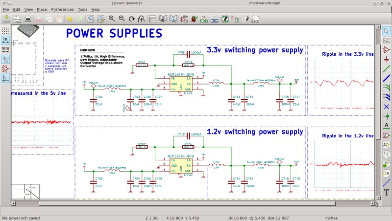
Allegro Design Authoring (also known as HDL), and OrCAD CIS are both schematic capture tools sold by Cadence. The partner PCB Software is called Allegro PCB Editor.
When it comes to differentiating features, Allegro Design Authoring (HDL) has two major benefits: it allows for managing PCB physical constraints in the schematic editor, which is very helpful for communicating complex constraint information.
Trace widths, spacings, groupings, and impedances can all be managed while capturing the schematic.
This tool also allows for parallel development, with multiple users editing the same file at the same time. That can be a huge help and save a lot of time for larger teams working to meet a critical milestone on a complex project.
When using CIS, the schematic capture tool is also capable of SPICE simulation. Allowing for simulation in a schematic capture tool can help to prevent errors by encouraging analysis.
For PCB layout, Allegro is a very capable PCB editor overall. It’s worth noting that some advanced features in Allegro require an additional license.
Nonetheless, if it fits into your budget, these tools (sometimes referred to as the Cadence suite) are capable of everything that any other EDA tool can do.
Altium
Altium is another popular tool, which has schematic capture and layout capabilities in one tool. This tool comes linked to an online component library, which is great for getting started.
It’s important to remember that using generic or global footprints for specific parts can lead to manufacturing issues, so make sure to verify each footprint is correct for your part.
This EDA tool also allows for SPICE simulation, and includes an Electro-Magnetics solver for accurate impedance and propagation delay calculations during PCB layout. Overall, Altium is a great tool that should meet the needs of many product designers.
KiCad
KiCad is another popular tool which combines schematic capture and layout in one tool. KiCad is the hardest EDA tool to describe in an article because it is still being developed.
That said, I will speak to the released version that is available today: 5.1.12. Be warned, there is a much awaited 6.0 release that adds a lot of features. As it stands, KiCad is free, open source, and cross platform.
It also ships with a standard component library, and supports many advanced schematic and layout techniques. It does lack some important features, especially for complex designs.
For example, there is no method for automatic length management of controlled impedance traces. It is not possible to have different intra-group and inter-group constraints for nets. Copper pours must be solid, rather than hatched shapes.
There is no EM solver, which means that propagation delay and length matching must be calculated with rules of thumb or an external tool. The lack of these features is serious enough that it could lead to additional hardware spins.
In addition, the export format of KiCad is currently limited to Gerber files, which may lead to additional effort when manufacturing.
Honorable Mentions
There are a few EDA tools that did not make an appearance in the above section. That is certainly not a disqualifier, because there are many capable EDA tools in the market.
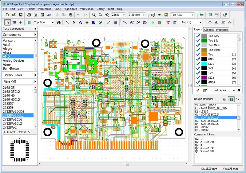
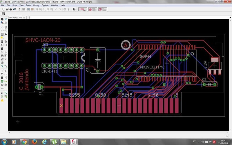
For example, DipTrace, EAGLE (now part of Autodesk Fusion 360), and PADS Professional. These are tools that I don’t know well because I haven’t used them extensively.
Some elements of EDA tools are subject to user preferences. Also keep in mind that using popular tools generally means that your tools will have an active community and be regularly updated.
Additional comments from John Teel: I find DipTrace to be one of the most intuitive to use EDA tools. However, it is not as popular as some of the other software packages. Eagle is one of my least favorite tools because it is very unfriendly to use; however, that may have improved since being integrated into Fusion 360. For more of my thoughts on DipTrace and Eagle please see this article.
Features and Recommendations
If you’re designing a circuit board that does not have a lot of controlled impedance routing, does not contain a lot of high-density routing and you’re working in a team of less than 4 hardware designers- KiCad is likely the tool for you.
It’s low cost and complementary libraries are excellent selling points. Manufacturing issues are risky when using the included library, but consulting with your PCB manufacturer and assembly house to maximize yield is a great management strategy.
For organizations that are designing more complex circuits with RF, high-speed digital, or sensitive analog components: Altium or the Cadence tools are both great choices.
As teams grow, and multiple users editing a single file becomes a critical feature, I need to recommend Allegro Design Authoring (HDL).
Conclusion
Choosing the right EDA tool is a difficult task. Thankfully, until you have a library of verified designs or existing products built in a specific tool, there isn’t a big difference from one to the next.
Through use of any of these tools, you’ll start to collect a group of verified schematic symbols and footprints, parts you know are correct and provide good manufacturing yields.
That’s when you might get locked in to using a specific tool, because change is painful and expensive. Recapturing symbols from one tool to another can be a tedious process.
Make sure to do your research and pick a tool that fits your budget and current needs, and that leaves room to grow with your business.

Hi John, I always appreciate these overviews! In 15 years of doing both software and hardware design, I have come to be skeptical overall of EDA tools. From a UI/UX perspective, they seem to lag years, sometimes decades, behind software in other domains. They will always be complex tools used to accomplish complex tasks, but other similarly complex software (i.e. mech eng software) proves that it is possible for complex tools to have much less friction (and fewer bugs!) than EDA overall. One example: using Orcad (Cadence) last year, I found that there were some basic PCB component placement tasks that were so onerous, it was fastest to open a command-line window and use text commands inherited from its 80s/90s origins. I haven’t used Allegro, so I can’t comment on that, but it sure seemed that Orcad was due for a bottom-up redesign. So it’s in the context of my overall dim view of the state of EDA software design that, in fairness, I have had to grudgingly appreciate some newer features of Altium Designer, introduced over the last 2-3 major revisions, that aren’t mentioned above (perhaps in favour of your also-appreciated brevity!). For readers who might factor this into consideration, Altium has introduced github-like cloud-based version control, on everything from an entire design to a single footprint. That same cloud-based platform incorporates a quite capable license-less viewer. When you need to show something to a client or a funder, they can log in, no cost to them or you, and gain read-only or comment-capable access to the schematic, pcb, and 3d model. Components, nets, and track segments can be searched, selected, and cross-probed. “Sticky notes” applied in the cloud viewer become visible in the desktop software, and vice versa, at the next push/pull. Threaded comments can mention users, and be open/closed. Even for a single user, being able to look back through the version history, compare changes, revert, etc is, I think, significant. The other feature that I think is worth mentioning, is Designer’s integration with the APIs of electronics distributors, especially in this time of supply chain troubles. From within a schematic, I can do an aggregate search on the distributors of my choice (say, Digikey Canada, Newark Canada, and Mouser) for, say, a 1pF capacitor, filter by footprint, then sort by price or availability (basically an integration of Octopart directly into the software). Any datasheet parameters that Digikey (etc) lists, are pulled directly into Designer, so I can often see the component’s properties (voltage rating, dielectric). Often the manufacturer has provided a 3d model, which is also attached, and sometimes even a symbol or footprint. Once I choose a component and drop it on my schematic, all of its properties and models come with it, as does a link to its datasheet. If I want to swap out the mftr-provided symbol for my own preference, I can do that without disturbing the other elements — but still use the earlier version if needed, because the component’s full… Read more »
Wow Mylene thank you so much for your in-depth comment and for sharing so much value with others! You definitely raise some good points to consider.
Cheers,
John
Happy to contribute. Thank *you* for moderating comments. I’ve converted several people to the way of Hardware Academy after one too many bad experiences on substack. 🙂
Thank you Mylene!!! I sure love hearing that you have referred people to the Hardware Academy!
EasyEDA deserves a mention too given it’s free (with ads) and while not quite as evolved as some others certainly can be very useful.
Thanks for the suggestion. I’ve not personally used EasyEDA before but I’ve heard it is a viable solution. I thought it limited you to only using EasyEDA for board production but I see they do offer (paid) the ability to output Gerber files. Thanks again for the comment.
Hey John, great article. We use Diptrace as it is cost effective and can be used for 99% or our projects. I have a Fusion 360 license and we will start testing their new schematic and PCB design software shortly. I am a big fan of Altium, but not the price tag. I will let you know how we like Fusion.
Thank you Stephan and I think Ryan did a great job too on this article. DipTrace is definitely my personal favorite but they all have tradeoffs. I’ll be curious to get your feedback on Eagle/F360, thank you.
Cheers,
John