
Guide to PCB Production & Manufacturing
Learn all the details of PCB production and manufacturing, including the most common types of materials used, and the main factors that will affect the price of your boards.
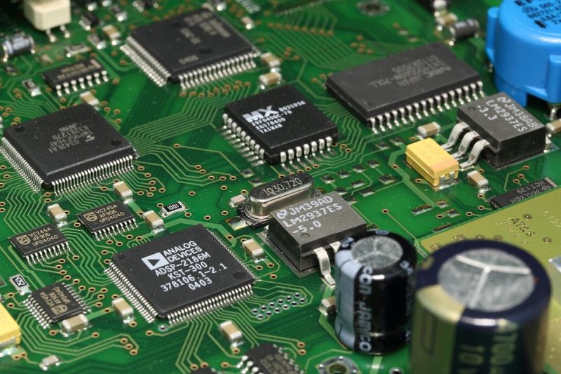
Cell phones, computers, microwaves, dishwashers, medical equipment, vehicle navigation systems, military equipment — these are just some examples of the many products that wouldn’t be able to function without printed circuit boards (PCBs).
There are lots of different types of PCBs — single layer, multi-layer, flex, rigid-flex, high frequency, among others — but the design, fabrication, and assembly of a PCB typically follows the same path, regardless of its type.
Keep reading for a detailed explanation of the PCB production and manufacturing process, including a discussion of all the common types of materials that are used and factors that will affect the price of your project.
Overview of PCB Manufacturing Process
A printed circuit board is an intricate, complicated project that requires specific guidelines, processes, and materials.
From beginning to end, the manufacturing process includes design and layout, fabrication, and assembly, all of which we’ll detail in this blog post.
Basic Parts of PCB Construction
The schematic diagram will dictate how your product can operate electrically. It also dictates the environmental conditions, like temperature, that you will need to adhere to.
The flex materials and PCB that you choose will be based on these parameters.
The schematic layout is a drawing that shows the board’s form factor and all the layers.
The basic parts of printed circuit board construction include:
Substrate — This term is used for any type of material that provides structural support to a PCB.
Copper — Since copper conducts electricity so well, it is used for a PCB’s signal traces.
Soldermask or coverlay — The soldermask technique coats most parts of the PCB in epoxy. You don’t coat any soldered electrical contacts, any fiducial markings, or any gold-plated terminals.
On flex, the coverlay serves the same purpose — to insulate the printed circuit board — but it has more flexibility and is more expensive.
Silkscreen — A silkscreen refers to digital printing, and though it doesn’t effect how a printed circuit board works, it’s worth mentioning when talking about construction.
A silkscreen will help you recognize warning symbols and identify components and where they should be placed.
More often than not, the ink will be the color white. You can switch to using black if you are working with a white colored substrate.
A silkscreen can identify many things, for example manufacturing marks, or test points. The ink is typically white, but black may also be used when the substrate is white.
Materials Used to Fabricate a PCB
It is important to select the right materials when fabricating your PCB. Let’s take a look at the most commonly used materials
FR4 — This laminate is flame resistant (NEMA grade) with a sub-layer of woven, glass fabric and an epoxy resin binder.
FR4 can operate in temperatures as high as 180°C. It has a poor CTE (coefficient of thermal expansion) and electrical properties, so it isn’t used a whole lot in PCB fabrication.
MEGTRON, Isola, and non-Teflon Rogers products — These materials are optimally used in products that need a fast signal speed and high signal integrity, which means they tolerate a wide range of temperatures.
PTFE (Teflon) — Often found in radar applications and various high-speed communication equipment.
Metal — The most commonly used metal in the fabrication of PCB boards is the highly conductive Copper.
PCB Manufacturing Process Steps
The process will vary depending on the type of board and technology used. For example, there are fewer steps with a double-sided board.
- Planning for computer-aided manufacturing (CAM). The first step entails setting up the board for manufacturing and placing multiple images on the board (called “step and repeat”).
The design review check (DRC) will confirm that the board is manufacturable and the Gerber files match the IPC net list.
- Is the board double-sided or multi-layer? A double-sided board does not have any lamination. The first place it goes is drilling.
- A multi-layer board goes to lamination.
- Multi-layer boards come out of lamination and go to drilling.
- Both double-sided and multi-layer boards go to electroless copper application after drilling.
- Photo resist lamination comes after electroless copper. The exposure of the image process is followed by the development of the image.
- Once the image is developed, the next step is electrolytic copper plating.
- After electrolytic copper plating, the panels go into an electroplated tin, which is the etch resist; they then go to the photo resist strip before undergoing the copper etch process.
- This is followed by etch resist stripping.
- LPI (Liquid Photo Imageable) solder resist is applied, imaged, and developed.
- Followed by legend application, which is a digital process much like an inkjet printer where the reference designators, serial numbers and other relevant information is printed on the board.
- Next is the electrical test, where 100% of boards are flying probe tested to the IPC 356 net list supplied by the customer.
- The milling of the boards out of the panel is the process where each board is mechanically milled out of the panel.
- The final inspection involves reviewing the boards along with the drawing requirements.
Design/Layout
Every PCB starts with design. This part is extremely important because multiple revisions to your design can seriously impede your timeline and completion of the project — ultimately costing you time and money.
Important factors during this process include:
Create the schematic. This refers to the design at the electrical level of the board’s purpose and function.
Use a schematic tool to capture the schematic for your PCB layout. Mentor PADS, Allegro, Altium, KiCad, Fusion 360, and DipTrace are popular options.
These tools show you exactly how your board will operate and where the components will be placed.
Design your PCB stackup. The stackup plays a role in how the mechanical engineer can design and fit the PCB into the device, as well as account for dielectric separation for controlled impedance requirements.
Define design rules and requirements. This step is usually dictated by standards and acceptability criteria from the IPC — the association for PCB and electronics manufacturing.
Place your components. In many instances, a PCB provider will discuss design and layout guidelines with the customer during placement of the components.
Insert drill holes. This step is driven by the components and a connection.
Route the traces. This refers to connecting segments of the path.
Add labels and identifiers. Including reference designators are helpful in showing where specific components will go on the PCB.
Generate design/layout files. These files contain all the information about your PCB. Once they are ready, you can begin fabrication and assembly.
Fabrication
During the fabrication stage, the printed circuit board takes shape and becomes a physical product.
Fabrication lead time will vary depending on the PCB provider and type of circuit board.
Standard rigid PCBs typically take 5-10 days and flex and rigid-flex circuits take 10-15 days. Some PCB providers may even offer 24-hour turnaround times.
Assembly
You have consigned, turn-key and partial options during the PCB assembly process.
A consigned assembly service is when you purchase all the parts on your own. Turn-key is when you let your PCB provider do everything that is needed.
You can buy the parts yourself (consigned) or allow the PCB provider to take care of everything for you (turn-key).
Factors That Affect PCB Cost
There are many factors that will affect the price of a printed circuit board. This is not an exhaustive list, but here are some of the most common:
PCB size — A PCB’s size, be it rigid or flex, will determine how many circuit boards can be placed per panel. This ultimately affects your per unit cost.
Number of layers — Each inner layer in a high-layer count PCB must undergo separate processing. Just remember that having lots of layers means you need more processing, which raises the cost.
The overall layer thickness and layer registration will also affect the price.
Flex material selection/weight — Certain material thicknesses (greater than 6 mil) require greater lead-times, and ultimately cost more.
Design complexity— Certain design features will drive up the cost. These include line spacing, line width, heavy copper weights, stacked and blind vias, lamination cycles, and coverlay types.
Certifications — Certifications may be required for certain projects, especially those in the government and military. Class 3 projects are often more costly, because they require tighter tolerances.
In addition, military certifications have to be current for any providers working on government-related projects, which is an added expense factored into the cost of a board.
Labor — More processes means more labor, which means a greater cost. There is a standard set of processes for every printed circuit board, but as PCBs become more complicated, additional ones may be required.
Conclusion
Manufacturing and fabrication of a printed circuit board isn’t simple or easy — but working with the right materials, the right technology, and most importantly, the right provider, can make all the difference.
And if there’s any part of the process that you’d like to know more about, just ask. Your PCB provider should be more than willing to provide assistance or answer your questions.
Written by Don Kaufman, Business Development Manager at Cirexx International. Don has worked in the PCB industry for 33 plus years, and enjoys sharing what he has learned about PCB layout, integrated circuit design, and laminate, chemical and equipment selection.
