
PCB Design: Making Your PCB as Small as Possible
When it comes to new hardware products many times smaller is better. One of the keys to a smaller hardware product is of course a smaller Printed Circuit Board (PCB).

Small size can be crucial for hardware products like wearable tech, as well as Internet of Things (IoT) products. So how do you achieve a smaller Printed Circuit Board (PCB)?
One technology for reducing PCB size that shouldn’t be overlooked if small size is critical for your product is the use of blind and buried vias. Their use allows the components on a PCB to be packed much tighter.
Vias are what connect traces between the various board layers. Standard through vias, which go through every layer of the board, actually reduce the routing space available even on the layers that don’t connect to these vias. Less available routing space means a larger board size.
This is where something called buried vias and blind vias come in to help eliminate this issue. A blind via connects an external layer to an internal layer, whereas a buried via connects two internal layers.
However, there are two issues with the use of blind and buried vias that designers need to consider.
The first isue with blind and buried vias is cost. Fabricating blind and buried vias is a more complicated process than a regular through via so they significantly increase the cost of the board.
The second issue with their use is that they have strict limitations on which layers they can be used to connect. To understand their limitations you must understand how the layers are stacked to make the board.
WARNING: If you don’t regularly design PCB’s this is about to get pretty complicated. Just warning you:)
Let’s start by looking at a 4-layer PCB with a layer stack-up as shown below.
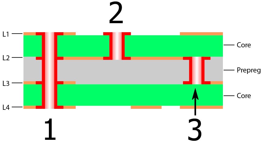
In this image, Via #1 is a classic through via, via #2 is a blind via, and via #3 is a buried via.
With this layer stack-up blind vias can only be used to connect L1 to L2, or L3 to L4.
Buried vias, on the other hand, can be used only to connect L2 to L3.
You can not use a blind via to connect L1 to L3, or L2 to L4. This is because the start and end of each via must be the far side of a core section to maintain structural integrity during drilling.
It gets even more complicated because instead of selecting a stack up of copper, core, copper, prepreg, copper, core, copper as shown above you can also select the stack up to be copper, prepreg, copper, core, copper, prepreg, copper.
With this layer stack-up blind vias can now be created to connect L1 to L3, or L2 to L4, but not L1 to L2 or L3 to L4.
Confused? Like I said the use of blind/buried vias can get really complicated.
The situation gets more complicated as the number of layers increases.
But regardless of the number of layers, just remember the most important rule: the start and end of each via must be the far side of a core section.
I find it best to draw the two layer stack-up options and then use the above rule to determine which layers can be connected using blind/buried vias with each stack-up.
Then you can decide which stack-up works best for your board design.
Just remember, in most cases it’s best to only use regular through vias. If you really want to push the size of a PCB as small as absolutely possible, then you should consider the use of blind and/or buried vias.

How would the via #3 get plated in that stackup in the image? Even if you drill the pre-preg, it needs a lamination cycle before it can go into plate and etch? But then it’s buried so it cannot be plated.
Perhaps that’s supposed to be core-PP-core, and the 1:2 and 3:4 are uVia?
Hi John
I am about to design a small six layer board and this article is very interesting. In your stack up diagram I can imagine how Vias 1 and 2 can be manufactured but I don’t see how Via 3 can be made. Is it possible to put a via in the prepreg before laminating the board? Or how can this be made? Would it be cheaper to limit yourself to through and blind vias and avoid buried vias? Thanks.
Yes Via #3 is predrilled in the prepreg. Blind and/or buried vias both drastically increase the cost. For 95% of the board designs I do only through holes are used. Blind/buried vias are generally only used when absolutely required to meet a certain size. Thanks for the comment Les!