
Teardown of an Amazon Echo Dot
In this article, I will teach you about product development by tearing down an Amazon Echo Dot, which is a great product to use as an example. The Echo Dot is an advanced tech product, yet it’s not so complex as to be completely overwhelming.

One of the best ways to learn about product development is to examine existing products on the market. Doing so can be a real eye-opener in regards to seeing absolutely everything that is involved in developing a new market-ready product.
This teardown is of the second generation Echo Dot which is significantly different from the original Echo Dot.
If you are unfamiliar with the Echo Dot it is a small voice-controlled speaker based on Amazon’s Alexa (voice command) service. You can ask the Echo to play music, answer questions, update you on the news, check the weather, set alarms, and to even control any compatible smart home devices.
The Dot’s big brother is the Echo. The biggest difference is the original Echo includes a much larger speaker and therefore has much better audio quality.
In this teardown we’re going to look at every single piece required for the Echo Dot, including the package, enclosure, and the electronics.
What’s included
The Amazon Dot consists of the paperboard retail box, a paperboard insert, the Dot itself, a USB plug with power adapter, two small instruction manuals, and three pieces of protective plastic coverings.
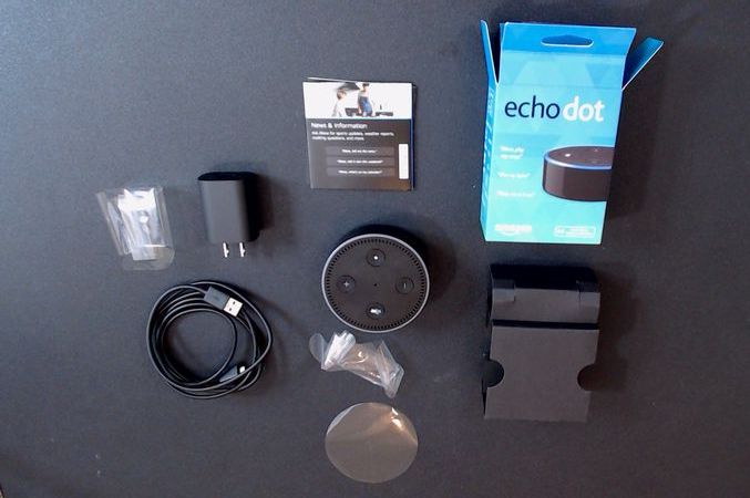
Everything that is included with the Amazon Echo Dot.
The retail package is a full-color box, with graphics and text printed on five sides. The box is made out of paperboard (thick paper as opposed to cardboard). It includes a peg hook for hanging in retail stores.
Then we have the inner insert that is also made of paperboard. It is designed to hold the various pieces and keep them separated. It is just one piece of paperboard folded and glued to make three different compartments to hold the Dot, the USB cord, and the USB power adapter.
Finally, the Dot and the USB power adapter are wrapped in protective plastic coverings to prevent scratching during shipment. These coverings obviously add very minimal cost (fractions of a cent).
The main reason I mention them is to highlight all of the little things involved in developing a market-ready product that may not occur to you. Although these coverings are a trivial expense, someone at some point spent a decent amount of time designing them so these little things shouldn’t be ignored.
Once you get past the packaging, the only components left are the Dot itself, the USB cord, and the USB power adapter. The USB cord and adapter is something that can be purchased off-the-shelf in high quantity, so it’s definitely not something you should consider designing yourself if needed for your own product.
Keep in mind that any product that plugs into a high-voltage AC outlet requires expensive UL certification. By purchasing a pre-certified power adapter you also will save yourself about $10,000 in UL certification costs if you plan to sell it in the U.S.
Finally, we get to the Dot itself which is what we will focus on for the rest of this article. The Dot includes a bunch of impressive technology. It obviously has voice recognition capabilities. It includes a Wi-Fi transceiver for communicating with the cloud (Amazon’s Alexa voice service). Most of the heavy duty processing is done on Amazon’s servers.
The Dot also includes a Bluetooth transceiver, an FM radio receiver, and a GPS receiver. It has four buttons: power, mute, volume up, and volume down. It has a ring of LED lights that illuminate when Alexa is listening (triggered by saying the word Alexa). It only includes two connectors: a 3.5mm audio out port and a micro USB port for supplying power.
Teardown of the Echo Dot
Let’s open up the Echo Dot and see what it took to develop this cool little product.
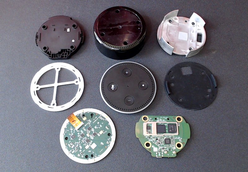
All of the internal parts making up the Echo Dot.
Non-slip pad
To take apart the Echo Dot we must first remove the non-slip silicone pad on the bottom of the unit which is attached via double-sided tape. After removing the non-slip pad, we have to remove a circular piece of transparent plastic which is also attached using double-sided tape.
From a manufacturing standpoint, dealing with glues can be quite challenging and messy, so it’s not something I recommend. Instead, the use of a double-sided adhesive tape is a much cleaner process.
Because of the simple circular shape of these two pieces they could probably be purchased from a supplier off-the-shelf without the need for any custom design on your part. Even if they don’t offer the exact diameter required the setup costs would be very minimal for custom size pieces.
Below the non-slip pad and transparent piece of plastic there are four Torx screws that hold the rest of the unit together.
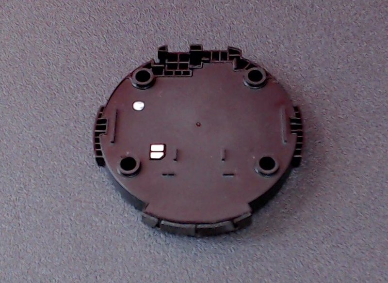
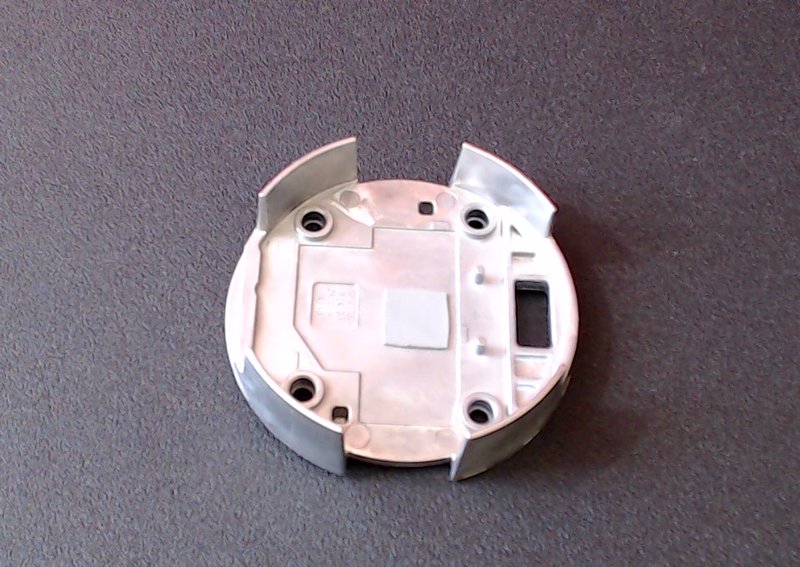
Primary plastic enclosure
The enclosure for the Dot, like most products, includes a top piece and a bottom piece.
The bottom piece (shown on the right in the image below) is rather simple. It consists of a single piece of injection molded plastic.
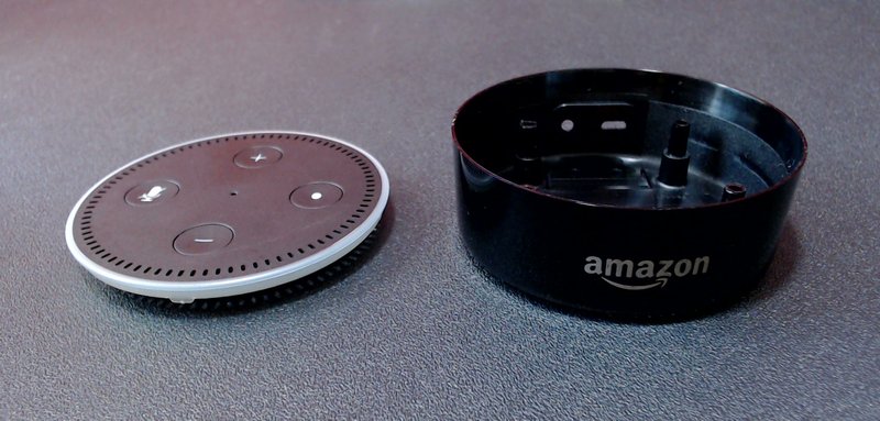
The plastic enclosure for the Amazon Echo Dot consists of a top piece and a bottom piece.
The top piece with the four buttons is a bit more complex. It’s made up of several different pieces of plastic including an odd looking shaped plastic piece that connects all the buttons and gives them some spring and holds them in place.
Custom shaped plastic piece which holds the four buttons and gives them some spring action.
The outer enclosure for the Dot is most likely a polycarbonate (PC) plastic. This tends to be the most popular type of plastic for higher-end electronic products.
ABS plastic is the other common type of plastic that tends to be more associated with use on toys and lower-end electronics. Polycarbonate has a much higher quality appearance than ABS, and it has a high impact strength, so if it drops, it doesn’t crack easily.
The speaker
The speaker used in the Dot is quite customized and probably doesn’t look like any type of speaker that you would recognize. The speaker itself is quite small but it is embedded in a custom plastic design which helps to amplify the sound coming from the speaker.
Speaker embedded in custom plastic enclosure to amplify sound.
The custom speaker enclosure looks like it’s made of at least two pieces of injection molded plastic.
The metal weight
Amazon has embedded a metal weight inside the Dot for two reasons. It gives the Dot some weight to make it feel higher quality, and it helps to prevent audio induced vibrations and rattling.
Production of a custom metal component such as this one will require a die-casting process. A die-cast is fundamentally very similar to a high-pressure injection mold used to produce plastic parts, except they are designed to work with molten metals instead of plastic.
This metal weight makes the Dot feel of a higher quality and prevents audio vibrations.
Spacers
We have a spacer ring which is plastic and goes in between the two printed circuit boards. Then you have a silicone rubber spacer that goes up against this plastic one and the purpose of this I suspect is to prevent audio induced vibrations.
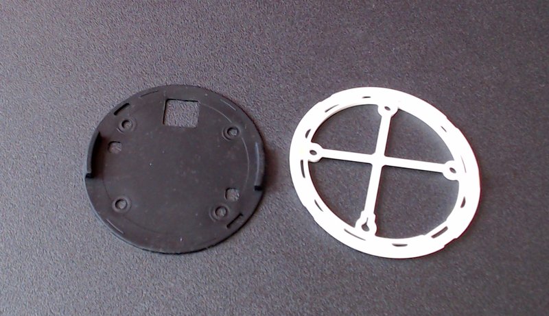
Spacers used between the two printed circuit boards. Black spacer is silicone, white spacer is plastic.
Printed Circuit Boards
Now we’re getting to the exciting part of the Echo Dot, where all of the action happens, and that is the electronics. The electronics for the Dot are on two separate printed circuit boards.
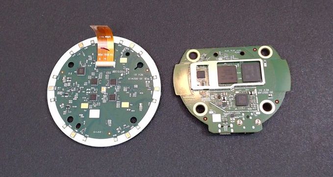
Two PCBs used in the Echo Dot. Microphone board on the left, processor board on the right
The first board is the microphone board which includes the microphones, LEDs, buttons, and analog-to-digital converters.
The second board is the processor board which includes the high-performance processor, the digital-to-analog converter which drives the speaker, and the WiFi/Bluetooth/FM/GPS functions.
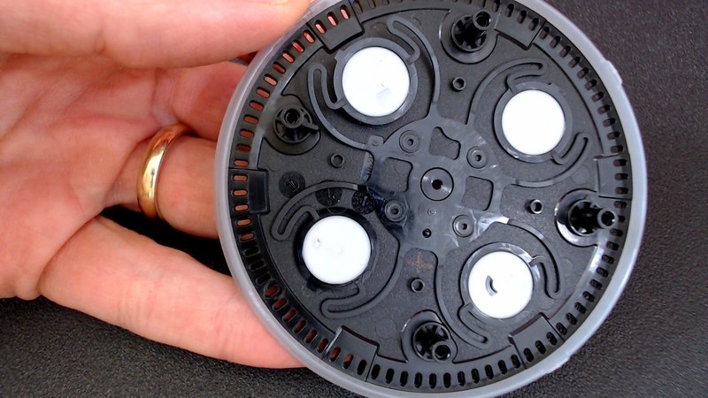
Microphone board
One side of the microphone board includes the microphones and LEDs, and the other side includes the four buttons. Let’s start by looking at the button side of this board which is shown below.
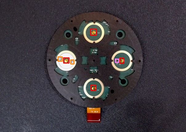
Microphone board showing the 4 tactile buttons (red), 2 LEDs (orange), and light sensor (pink).
The four buttons on the PCB are low-cost dome tactile buttons. The physical part of the buttons that we looked at already on the enclosure includes a bump that pushes down on these tactile buttons when pressed.
The button on the left side in the image above is the mute button which is illuminated when turned on. You’ll notice two very small LEDs right next to that tactile button. The white background on this button helps to ensure the light is reflected outward.
On the right side is the power button. You’ll notice just to the left of this button is a very tiny component. That’s a light sensor that allows the Echo Dot to detect the amount of light in the room. Based on the light in the room, it adjusts the brightness of the LEDs that are on the other side that illuminate a ring around the Dot.
That’s pretty much all there is on this side of the board, just the four dome tactile switches, two LEDs and a light sensor.
On the other side of the board, we have the seven microphones in total with six located around the perimeter, and one in the very center of the board.
Also, along the outside you have the RGB LEDs. You’ll notice there are two LEDs around each of the six perimeter microphones. These LEDs illuminate the outer ring of the Dot to either let you know that Alexa is listening, an alarm is going off, etc.
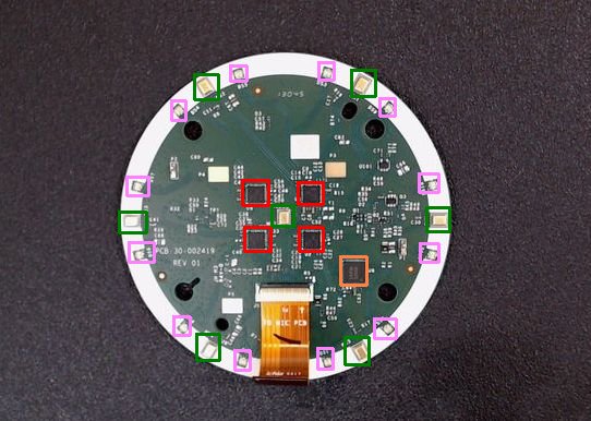
Board with microphones(green), LEDs (pink), Analog-to-Digital converters (red), and LED driver (orange).
In the center of the board you have four analog to digital converter (ADC) chips. They take the analog signals coming from the microphones and convert them to a digital signals that can be processed.
These A/D converters are the TLV320ADC from Texas Instruments. Each one of these is a two-channel analog to digital converter. Since the Dot has seven microphones, four of these converter chips are required. One converter has an unused channel.
Just below and to the right of the four converters you’ll see another microchip. There is no part number on this chip so it’s difficult to find the details on it. Many times manufacturers won’t put the part number on microchips partially because they want to prevent reverse engineering of their product.
Some things I’ve read claim this is a microcontroller. I tend to think it’s more likely an LED driver, or some combination of these two functions.
Of course, there are a lot of other small support components including resistors, capacitors, and a few discrete transistors. Although critical for functionality, these components usually add very little cost.
Processor Board
Now we’re going to look at the mainboard. Let’s start with the backside of this board which includes primarily just the three connectors (ribbon, USB, and audio out) and the digital-to-analog converter (DAC).
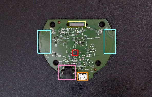
Backside of the processor board showing the DAC (red), microUSB connector (orange), audio port (pink), ribbon cable connector (yellow), and WiFi/Bluetooth/GPS PCB antennas (cyan).
The Dot takes analog audio from the microphones, converts that to digital format, processes the digital data, then outputs digital audio data which is then converted back to analog via the DAC chip shown toward the center on this side of the processor board.
The DAC chip is the TLV320DAC from Texas Instruments. In addition to the digital to analog function the TLV320DAC also includes an embedded speaker amplifier. The output of this chip then feeds into the speaker.
On each edge of this side of the board are two PCB antennas which are used for the WiFi, Bluetooth, and GPS functions. PCB antennas are always the cheapest type of antenna since they require no additional components. However, they are tricky to design correctly so I usually recommend using ceramic chip antennas instead, at least initially.
This board also includes the micro USB connector and the audio output port which are both soldered right onto the PCB. When this board is placed in the enclosure these two connectors align with the appropriate holes in the enclosure.
There are two ways to typically handle connectors that users must access. The simplest option is to mount them directly on the PCB just like Amazon has done with the Dot.
The other option is to use wired connectors which gives you more flexibility in the placement of any external connectors. The downside is this option requires additional manufacturing steps to solder the wires onto the board and to manually place the connectors in the correct enclosure slots.
Wired connectors give you more placement flexibility but they add more assembly complexity.
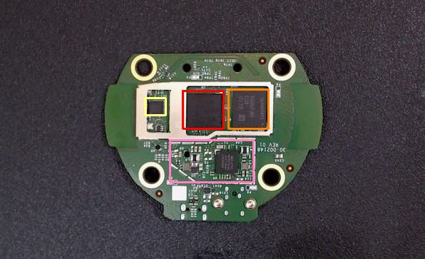
Board with processor (red), memory (orange), wireless chip (yellow), and power management circuit (pink).
Finally, we get to the brains of the Dot which are found on the other side of the processor board. The processor, memory, and wireless chip are all inside a metal shield.
This shield serves two purposes. It prevents the high-speed components from radiating out electromagnetic interference which can complicate FCC certification. Secondly, it prevents any outside noise from causing interference with these components. The wireless chip is shielded separately from the processor/memory chips otherwise the processor noise would interfere with the wireless functionalities.
We have four primary chips on this side of the board: the processor, the memory, the wireless analog front-end, and the power management IC.
The processor chip is the MediaTek MT8163. It’s a quad Cortex-A53 processor running at 1.3 GHz. It also includes the Wi-Fi and Bluetooth transceivers, an FM receiver, and the GPS receiver.
The memory chip is from Samsung and provides 4 GB of Flash memory and 512 KB of high-speed DDR3 SDRAM memory for temporary storage.
The third chip under the metal shield is the wireless analog front-end chip. This chip is the MT6625LN from MediaTek. I’ve seen other teardowns of the Echo where they have referred to this chip as having the wireless transceivers and receivers. That’s actually not correct.
The transceivers and receivers themselves are embedded in the MediaTek processor chip. This separate wireless chip is only the analog front-end for these four wireless functions. It basically consists of filters, amplifiers and RF switches for the four wireless functions.
The final chip is the power management IC which is the MediaTek MT6323. It provides all the various voltages required for all the components on both of the boards. It includes three buck regulators and 23 linear regulators.
A buck regulator is a type of switching voltage regulator that can take a higher voltage and step it down to a lower voltage. It does this very efficiently without wasting power, but it also tends to be more complicated than a linear regulator.
A switching regulator can generate considerable high-frequency noise. Because this circuit is so close to the processor and wireless chip it’s especially critical that Amazon has placed a shield around those components.
The most complex chips used in the Dot are from a Taiwanese semiconductor company called MediaTek. This is considerably different than the original Dot which, for example, used a digital media processor from Texas Instruments as the primary processor.
I suspect Amazon switched to MediaTek chips in order to reduce the manufacturing cost and increase their profit margins.
Conclusion
As you can see, the Amazon Echo Dot is a very efficiently designed product. It makes a very good product to use as an example of how to develop a state-of-the-art, market-ready, electronic product.
Regardless of your technical experience, I highly suggest doing your own teardown on a competing product that is similar to the product you wish to develop. You don’t need to be able to understand the function of every microchip in the design, but doing a teardown will give you immense insight into what it will really take to develop your product.
If you enjoyed this teardown and would like me to do more of them then please share this article or leave a comment below.

Great article! would like to see more of such articles.
Great teardown! One question: in the speaker photo, what part is the actual speaker? the photo shows what look like two contacts and one white rectangle embedded in a large membrane. Is that membrane the vibrating part of the speaker, or is that hidden?
how many linear regulated outputs?
Hi Andrew,
I’m not quite sure and that’s difficult to determine with the schematic, or some serious reverse engineering of the electronics. I didn’t got into that much detail.
John
Thank you so much for this John. Will be a member soon
Hi Prateek,
Thank you for the comment. I look forward to helping you further in the Hardware Academy. You can join at any time.
Cheers,
John
Nice non-destructive teardown. It’s very useful to understand how things work, how they are constructed, and what the vendor had in mind. Sometimes big surprises show up. Like unpopulated footprints (same PCB on multiple products?), presence of embedded OEM modules that you can buy too, etc.
The next step would be a destructive analysis. This allows an accurate cost estimate of the whole system. E.g. by cross-sectioning a PCB you can count layers, copper thickness, measure vias and other features, and quote it.
Decapping chips is also very helpful, even if you don’t intend to design an ASIC. Here are a few examples:
– chips may be unknown because the package is unmarked. But the dies usually have an id, brand or logo etched somewhere. This is extremely informative.
– by just measuring the chip size and having a moderately magnified top view (x25 is more than enough) you have an idea of what it does. In the case of the unknown chip here it would be straightforward to discriminate an MCU against an led driver.
– one step further: identifying the process node lets you know how much the chip costs quite accurately. Very useful with unknown chips, but also with known references that you can’t get quoted because you just don’t qualify (some popular brands are famous for that.)
Awesome comment Hardy, thank you!
Great article. Small word of correction: 1.) UL certification is not actually required by law on any product sold in the United States. It’s just a very good idea, for example for insurance purposes and for opening your market to a wider audience, some of whom will refuse to buy without certification, such as schools or businesses. 2.) It’s not even necessary to go with UL. Any Nationally Recognized Testing Laboratory (NRTL) will suffice. There are many NRTLs; UL is just the most well known. So if you can save money going with another lab and your customers will accept that, you have that as an option.
Great points Christopher! Thanks for sharing.
John
Interesting teardown, thanks
Thanks Gabriel!
Very nice post and “tearing down” is a very interesting approach.
It might be a little bit more difficult but I’m looking forward to see a tear-down of a IC or more specifically a MCU.
Looking forward to checking your next post.
Thanks for the comment. Teardown of an IC is definitely more complicated. I don’t have the necessary equipment to be able to access the chip inside an IC package. You also need a very good microscope with camera. Also no one (except chip makers) really designs their own chips so it would be of limited use for most of my readers.
Decapping (dissolving the epoxy package) an IC can be done relatively easily, with a Dremel and nitric acid (which can be made from nitrate-based fertilizer). You make a hole with the Dremel, place the nitric acid over it and heat it until the epoxy dissolves. Then you can inspect it with a $50 microscope with camera which you can easily buy at Chinese stores.
That being said, unless you need an ASIC for your product, you’re not going to do anything of the above. And if you need an ASIC, you also need a lot of money anyways.
Nice Tear Down. That MediaTec chip set is very impressive, 4 ARM cores, and all of the communication devices.
Just for reference, what would you estimate your design cost to build something like this?
Great video John! Really helpful. Looking forward to your teardown of the echo 3. I really appreciate the high def photos next to the video. Keep up the great work, I will be following you.
Thank you Menno! I appreciate your feedback. I definitely want to do more of these teardowns and I feel they are one of the best ways to learn about product development.
Brilliant post! Super informative. While I scrolling through the chronology of your breakdown, I couldn’t help but wonder what would it cost for the average product developer to create this product if they invented Amazon Echo before Amazon did?
In other words, all production costs and prototyping aside, if an independent product developer created a production-quality prototype and sent it off to a manufacturing company for pricing of 1000, 10000, and 100000 units, would costs run for parts and assembly?
Keep up the great work!!!
Thanks Will for your comment, I’m really happy you enjoyed this article!
I’m a little confused by your question though. You say “all production costs aside…” then ask what it would cost to manufacture it at various volumes. Did you mean to say all “development costs aside”? I assume you are asking for the production cost and not development costs.
It definitely wouldn’t be as cheap for a small company to produce. Amazon is obviously able to demand the best pricing.
Thanks again!
John
Very nice and good excellent descriptions . congratulations
A small constructive criticism on the video, you should have some zoom to the boards when you point out to small components. Its very hard to see.
Any way i learned a lot and will continue following your blogs
Thank you Carlos! I appreciate the feedback and suggestion. I’m still a bit new to video and I will continuously work to improve the quality including zooming in when necessary.
This is very helpfull for those who electronic design and testing . i got lot of idea how to work with ADC and DAC , Can you explain which way more help full by using as IOT tool